
Development of ZnTe film with high copper doping efficiency for solar cells
2022-10-26 09:54:06XinLuLin林新璐WenXiongZhao趙文雄QiuChenWu吳秋晨YuFengZhang張玉峰HasithaMahabadugeandXiangXinLiu劉向鑫
Chinese Physics B 2022年10期
Xin-Lu Lin(林新璐) Wen-Xiong Zhao(趙文雄) Qiu-Chen Wu(吳秋晨)Yu-Feng Zhang(張玉峰) Hasitha Mahabaduge and Xiang-Xin Liu(劉向鑫)
1Institute of Electrical Engineering,Chinese Academy of Sciences,Beijing 100190,China
2University of Chinese Academy of Sciences,Beijing 100049,China
3Georgia College and State University,Milledgeville,GA 31061,USA
4Institute of Qilu Zhongke Electrical Advanced Electromagnetic Drive Technology,Jinan 250101,China
Keywords: solar cell,radio frequency sputtering,doping efficiency,post-deposition heat treatment
1. Introduction
Now,the technology of making cadmium telluride(CdTe)solar cells is one of the key technologies in the field of thin film solar cells.[1–3]CdTe back contact material for cadmium telluride (CdTe) cell has always been a significant research direction.[4]For a solar cell with traditional structure(Fig.1(a)),a hole barrier is formed in back contact due to mismatch of work function.[5,6]Many researchers have proved that copper-doped zinc telluride (ZnTe:Cu) is an ideal back contact material(Fig.1(b)).[7,8]The ZnTe:Cu is a hole transport material that is inserted between electrode layer and absorber, which can reduce the valence band discontinuity(0.05 eV–0.30 eV)caused by the contact barrier.[9]Owing to the slight mismatch of lattice between ZnTe:Cu and CdTe,the ZnTe:Cu film can be used as an electron back reflection layer(1.00 eV–1.08 eV)to inhibit interface recombination.[10]After the activation of post-deposition heat treatment(PDHT),high level carrier concentration can be easily achieved.[11]

Fig.1. Schematic diagram of energy band structure for CdTe solar cell(a)metallic contact,and(b)modified cell with ZnTe:Cu layer.
Although there are few reports on RF coupled DC sputtering of ZnTe:Cu film,there may exist an effect on film properties as demonstrated on ZnO:Al and Cd2SnO4.[12,13]In this work, we investigate the influence of target bias and PDHT for ZnTe:Cu. Furthermore,a systematic study is conducted on the devices with different contact materials,which proves that ZnTe:Cu back contact layer may reduce hole barrier. Through effective activation process, the efficiency of solar cell is improved by the modified band alignment.
2. Experiment
2.1. Preparation of ZnTe:Cu and devices
ZnTe:Cu films were prepared on Corning 7059 glass substrates through RF-coupled DC sputtering followed by rapid thermal processing (RTP) at different temperatures.[14]Optimized ZnTe:Cu films were then used to complete CdTe solar cell devices. Both CdS:O and CdTe polycrystalline films were sputtered on the commercial TEC15 substrate by using standard process. Afterwards, the CdS:O/CdTe devices were activated by chloride treatment, which was conducted in mixed atmosphere with 5% oxygen and 95% nitrogen.[15]After the chloride treatment,different back contacts were used(Fig.2).
For reference, the Au electrode (30-nm thick) or Cu/Au bilayer structure with an optimal Cu thickness (4 nm) was evaporated on an activated absorber surface by electron beam evaporation (Figs. 2(a) and 2(b)). As shown in Fig. 2(c),ZnTe:Cu/Au stacked structure was sputtered on an absorber layer. The ZnTe target with three inches in diameter was used,which has a purity of 99.99%with 5%atomic concentration of copper. The devices with different thickness ZnTe:Cu buffer layers(40 nm–200 nm)were annealed on the RTP furnace at 200°C–320°C for 20 s–120 s.
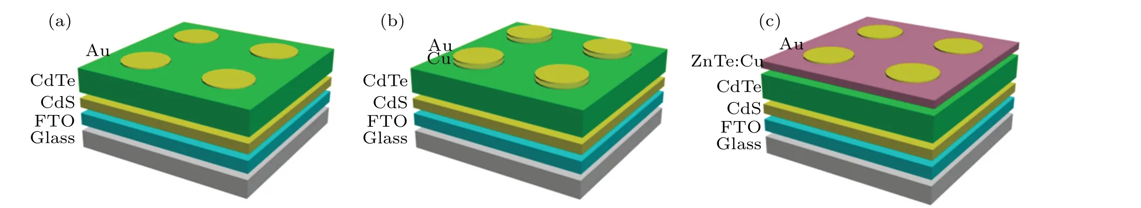
Fig.2. Schematic diagram of devices with different contact layers: (a)Au,(b)Cu/Au,(c)ZnTe:Cu/Au(nonscaled).
2.2. Characterization methods
The morphology of film surface and device cross section were observed by using scanning electron microscope(SEM,Zeiss Sigma). The film electrical property was measured by Hall effect(Nanometric Hall 5500). The atomic ratio was investigated by energy dispersive spectrometer (EDS, Bruker).For the device, the current density–voltage (J–V) curve was measured on a source meter (Keithley 2400) and solar simulator (Newport Oriel 91159A, USA). External quantum efficiency (EQE) was investigated in PV measurement (QEX7 system,USA).The capacitance–voltage(C–V)was measured in a semiconductor characterization system (SCS, Keithley 4200).
3. Results and discussion
3.1. Improvement of doping efficiency
Deposition rate, optical and electrical properties of ZnTe:Cu film are affected by target bias voltage as demonstrated in previous work.[14]The influence of PDHT and target bias are investigated to understand benefits obtained from RF-coupled DC sputtering and heating process separately.The combined process of PDHT (300°C) and target bias voltage(-122 V)is dramatically improved,which makes the resistivity decrease from 243.58 Ω·cm to 0.04 Ω·cm(Fig.3(a)). The carrier mobility is enhanced to 0.214 cm2/(V·s) (Fig. 3(b)).As shown in Fig. 3(c), the carrier concentration is improved from 5.0×1017cm-3to 9.2×1020cm-3at a-122 V bias voltage and RTP at 270°C for 60 s. Nevertheless,the carrier concentration decreases with excessive annealing temperature increasing. The doping efficiency is computed as the ratio of free hole density to copper concentration,showing an upward trend from 0.03% to 60.9% (Fig. 3(d)).[16]The copper concentration in ZnTe:Cu film is derived from the relative ratio of Zn to Te to Cu from EDS data taken from the same film.The doping efficiency can be correlated with the performance for CdTe-based solar cell.The higher doping efficiency means that more copper atoms substitute for Zn sites in ZnTe lattices and there remain less mobilized copper atoms which can enter into the CdTe absorber layer. Copper is suspected as a dominant element for CdTe-based cell degradation.[17]Possible degradation mechanisms include the decline in window layer transmission (decreasedJsc) and change in the space charge region(decreasedVoc).[18]
As shown in Table 1, in National Renewable Energy Laboratory, Gessertet al.noted that carrier concentration of ZnTe:Cu(0.45 at.%)film is 1.9×1018cm-3at annealing temperature of 375°C in flowing N2for 30 min.[19]And the asdeposited ZnTe:Cu (6 at.%) film reaches a maximum carrier concentration of 3×1020cm-3at a substrate temperature of 300°C.[20]In the University of Toledo,Bohnet al. noted that the ZnTe:Cu(8.86 at.%)film with a high carrier concentration of 1×1021cm-3is grown at 400°C.[21]In our laboratory,the doping efficiency of ZnTe:Cu(5 at.%)film (200 nm thick) is improved to 60.9%.
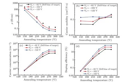
Fig.3. ZnTe:Cu properties with different target bias of-82 V(black line),-102 V(red line),and-122 V(blue line):(a)resistivity,(b)carrier mobility,(c)carrier concentration,(d)doping efficiency.
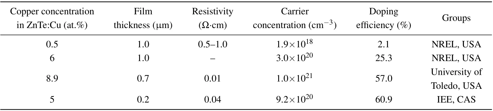
Table 1. Summary of electrical performance of ZnTe:Cu films deposited by different groups.
3.2. Fabrication of CdTe solar cells
To understand the changes of back contact materials,it is significant to review the fabrication of device with fundamental structure.All solar cells are deposited on NSG TEC15 glass which is coated by SnO2:F(FTO)(Fig.4(a)). The CdS:O film is sputtered through RF deposition process and used as a window layer on the TEC15 glass for solar cell(Fig.4(b)). Then polycrystalline CdTe film is deposited on CdS:O film in the same sputtering system with a substrate temperature of 301°C(Fig. 4(c)). With the achievement of chlorine activation process,the study of the CdTe grain boundary surface by SEM reveals that the CdCl2treatment results in the enlargement of the grain size(Fig.4(d)). As for back contact,the interface issue of the mismatch of work function can be solved by inserting a buffer layer of ZnTe:Cu which is prepared by the RF coupled DC sputtering, and device performance is significantly enhanced after being annealed additionally. Figure 4(e)shows that the surface of CdTe film is homogenously covered with uniform ZnTe:Cu film. Figure 4(f) shows the surface morphology of ZnTe:Cu with optimal RTP. After the PDHT, the grain boundaries become blurred where the small grains are“swallowed”by large grains.
The superstrate structure is used for CdTe solar cells as shown in Fig.5(a). Figures 5(b)–5(d)show the box plots obtained from 36 cell efficiencies for each condition. The active area of each cell is approximately 0.07 cm2. Figure 5(b)shows the effect of ZnTe:Cu thickness with RTP at temperature 300°C in 100 s.The cell with 80-nm-thick ZnTe:Cu layer reaches a best performance (10.55%, in average), which is mainly due to the enough copper atoms needed to enhance the p-type doping concentration of the absorber layer. Figure 5(c)shows the efficiency(Eff)valuesversusthe annealing temperature for devices with 80-nm-thick ZnTe:Cu layer and annealing time of 100 s. “No RTP”samples refer to the devices that are unannealed. When the annealing temperature is 280°C,the maximum solar cell efficiency is obtained(11.63%,in average). Figure 5(d) displays the statistical results of the performance for devices with 80-nm-thick ZnTe:Cu film and the same annealing temperature (280°C). TheEffvalue first increases from 8.78%(20 s)to 12.89%(60 s)and then decreased(9.53%,120 s).
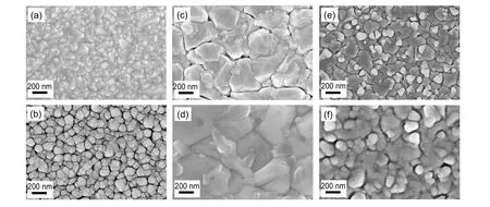
Fig. 4. SEM image of (a) FTO, (b) FTO/CdS:O, (c) FTO/CdS:O/CdTe (as-deposited), (d) FTO/CdS:O/CdTe (with Cl treatment), (e)FTO/CdS:O/CdTe/ZnTe:Cu(as-deposited),and(f)FTO/CdS:O/CdTe/ZnTe:Cu(with optimized PDHT treatment).
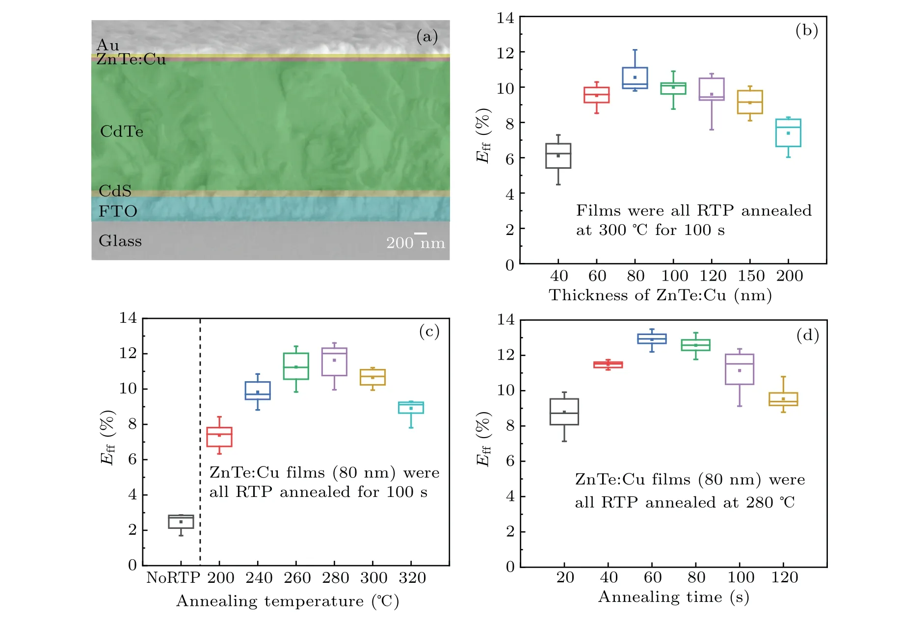
Fig.5.(a)Cross section of device,(b)effect of ZnTe:Cu thickness on device efficiency,(c)effect of annealing temperature on device efficiency,and(d)effect of annealing time on device efficiency.
Figure 6(a) displays the typicalJ–Vcurves for devices with respective contact materials of Au, Cu/Au, ZnTe:Cu/Au with No RTP treatment,ZnTe:Cu/Au with optimal RTP treatment at 280°C for 60 s,and ZnTe:Cu/Au with excessive RTP treatment at 320°C for 100 s.We collect the highest efficiency of CdTe-based film solar cell under different preparation conditions. The corresponding photovoltaic measurements of devices are summarized in Table 2.
The typical CdTe soalr cell with Au contact material shows the behavior of“roll-over”,which causesFFof 51.51%andVocof 606 mV. The efficiency value of this device is 7.27%, withJsc= 23.21 mA/cm2,Rs= 9.69 Ω·cm2, andRsh=350 Ω·cm2. The behavior of“roll-over”implies the existence of contact barrier,which results from the mismatch of work function between electrode layer and absorber layer.[22]With the incorporation of a copper film,FFandVocexhibit a limited improvement of 65.36% and 736 mV, withRs=5.40 Ω·cm2andRsh=1675 Ω·cm2. TheJscvalue remains essentially unchanged (23.68 mA/cm2), and thus the overall efficiency increases to 11.48%. As for ZnTe:Cu contact material, as-deposited solar cell with no RTP treatment shows bad current collection(18.41 mA/cm2). The device efficiency is 2.87%, leading to lowVoc(508 mV), the high series resistanceRs(21.26 Ω·cm2),the low shunt resistanceRsh(86 Ω·cm2), and fill factor (30.65%). After the optimal RTP treatment,the performance of device is significantly enhanced.TheRsdecreases from 21.26 Ω·cm2to 4.23 Ω·cm2because of the barrier reduction.[23]The leakage of electricity is prohibited andRshimproves from 86 Ω·cm2to 1109 Ω·cm2. At the same time, theJ–Vcurves exhibit no “roll-over” behavior, withEff=13.48%,Jsc=26.76 mA/cm2,Voc=756 mV,andFF=66.60%. Once the devices are over treated with excessive annealing temperature or annealing time, all the photovoltaic parameters obviously decline. For example, the efficiency of cell declines from 13.48% to 9.55% (29.15% in decrement), withVoc= 730 mV,Jsc= 25.59 mA/cm2, andFF=51.10%. The degradation is assumed to be mainly because of copper diffusion to CdS:O film, which degrades the PN junction and leads to shunting.

Fig.6. (a)The J–V curves and(b)EQE–wavelength curves.
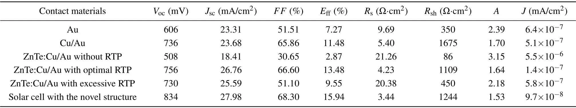
Table 2. Photovoltaic parameters of different devices.
As shown in Fig. 6(b), the values of EQE decrease at wavelengths above 600 nm for the device without Cu(with Au electrode only).Similarly,EQE spectrum shape of device with Cu/Au contact material shows a downward trend in a wavelength range of 600 nm–800 nm. Specific to the ZnTe:Cu/Au back contact device with optimized RTP treatment, the EQE spectral keeps relatively stable over the same wavelength range of 600 nm–800 nm without decreasing. In general, because of free carrier recombination near the back contact,the EQE response decreases at long wavelengths.[24]In contrast,the conduction band barrier of device with ZnTe:Cu/Au contact material has an effect on the EQE response,which works as free electron barrier and reduces the recombination rate of free carrier.
To obtain higher conversion efficiency, we prepare CdTe-based solar cells with a novel structure of Cd2SnO4(CTO)/MgZnO (MZO)/CdTe/ZnTe:Cu/Ni. The CTO film(200 nm)is used as the conductive layer instead of FTO film to improve the electrical properties and transmission of TCO layer.[13]The MZO film (80-nm thick) is used as the window layer instead of CdS film to enhance the response of solar cell at short wavelengths.[25]The CdTe absorber prepared by closed space sublimation (CSS) at high temperature replaces the method of magnetron sputtering at low temperatures. In addition,the use of Ni as the back electrode instead of Au can reduce the production cost of solar cells.
Figure 7(a) displays theJ–Vcurve for the best device with contact materials of ZnTe:Cu/Ni. TheJ–Vcurves exhibit no “roll-over” behavior, withEff=15.94%,Voc=834 mV,Jsc=27.98 mA/cm2,FF=68.30%,Rs=3.44 Ω·cm2, andRsh=1244 Ω·cm2. Figures 7(b)–7(d)show the box plots obtained from 36 cell efficiencies under the different conditions of ZnTe:Cu film. Figure 7(b) shows the effect of ZnTe:Cu thickness with RTP at 260°C for 40 s. The cell with 90-nmthick ZnTe:Cu layer reaches the best performance (13.09%,average). Figure 7(c)shows the comparison of annealing temperature among devices with 90-nm ZnTe:Cu layer and annealing time of 40 s. When the annealing temperature is 290°C, the maximum solar cell efficiency is obtained to be an average of 14.00%. Figure 7(d) displays the results of performance for devices with 90-nm-thick ZnTe:Cu film and the same annealing temperature(290°C).Therefore,ZnTe:Cu back contact layer with a thickness of 90 nm annealed at 290°C for 40 s can achieve the best conversion efficiency for the devices with novel structure.
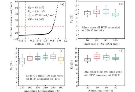
Fig.7. (a)The J–V curve, (b)effect of ZnTe:Cu thickness on device efficiency, (c)effect of annealing temperature on device efficiency, and(d)effect of annealing time on device efficiency.
3.3. Analysis of J–V and C–V for solar cell
With regard to the characteristic ofJ–Vbehavior, the most important thing is the prevalence of parasitic losses,which can be commonly described by the following diode equations:[24,26]

whereJandJLare the reverse saturation current and photogenerated current,respectively.
The CurVA 2.0 software is used for the numerical analysis ofJ–Vplot. Figure 8(a) shows theJ–Vplots for device with efficiency of 15.94%. This includes sufficient data in the first quadrant and third quadrant where non-ideal effects are not described by Eq.(1), such as current blocking behavior, which are commonly observed in solar cells. Figure 8(b)shows the derivativeg(V) with respect toVin a reverse bias voltage region where derivative of diode term in Eq. (2) becomes negligible. In this case, theg(V) curves reveal thatG(dark)=0 mS/cm2andG(light)=0.9 mS/cm2. In addition,the slope of realisticJ–Vcurve is very small in the range of reverse bias, so there will be some noise in calculating the derivative under illumination condition. Figure 8(c)shows the dV/dJ versus(J+JscGV)-1plot, which will yield a line ifJLis independent of voltage. From the dark data or the linear region of light data, an intercept is obtained for the series resistance(Rs=3.44 Ω·cm2)and a slope is calculated for diode ideality factor (A=1.53). Figure 8(d) shows semilogarithmic plot of (J+JscGV)versus(V-RsJ). According to dark data or the linear region of light data, the current indicates that the intercept gives the diode reverse saturation current(J=9.7×10⁻⁸mA/cm2). The slope is equal toq/AkT,so the diode ideality factor(A)can be calculated to be 1.53(A=1.53)which is consistent with the value indicated in Fig. 8(c). In addition, the values ofAandJfor all devices with different preparation conditions are summarized in Table 2 for comparison. When Cu/Au layers, ZnTe:Cu/Au layers with optimal RTP and ZnTe:Cu/Ni with optimal RTP are used for the back contact of solar cells, the corresponding diode quality factors are 1.70, 1.64, and 1.53, respectively. The results of ideality factor between 1 and 2 indicate that the device operated with dominant trap states is the recombination in space charge region. When Au monolayer, ZnTe:Cu/Au layers without RTP and ZnTe:Cu/Au with excessive RTP are used for the back contact of solar cell, the corresponding diode quality factors are 2.39,3.15,and 2.18,respectively. When the value of diode ideality factor exceeds 2, the interface and tunneling recombination additionally contribute to the total recombination.[26]This suggests that the better quality absorber layer is necessary for high performance.
To obtain free carrier densities and depletion widths from the PN junction of device,C–Vprofiling is carried out at room temperature(Fig.9(a)).The carrier concentration is calculated from the following equations:[27]

whereC(V) is the capacitance per area, ΔQthe incremental depletion charge with an applied voltage ΔV,εthe permittivity of the CdTe,Wthe depletion width,qthe electron charge,N(W)the space charge density,andVDthe diffusion voltage.
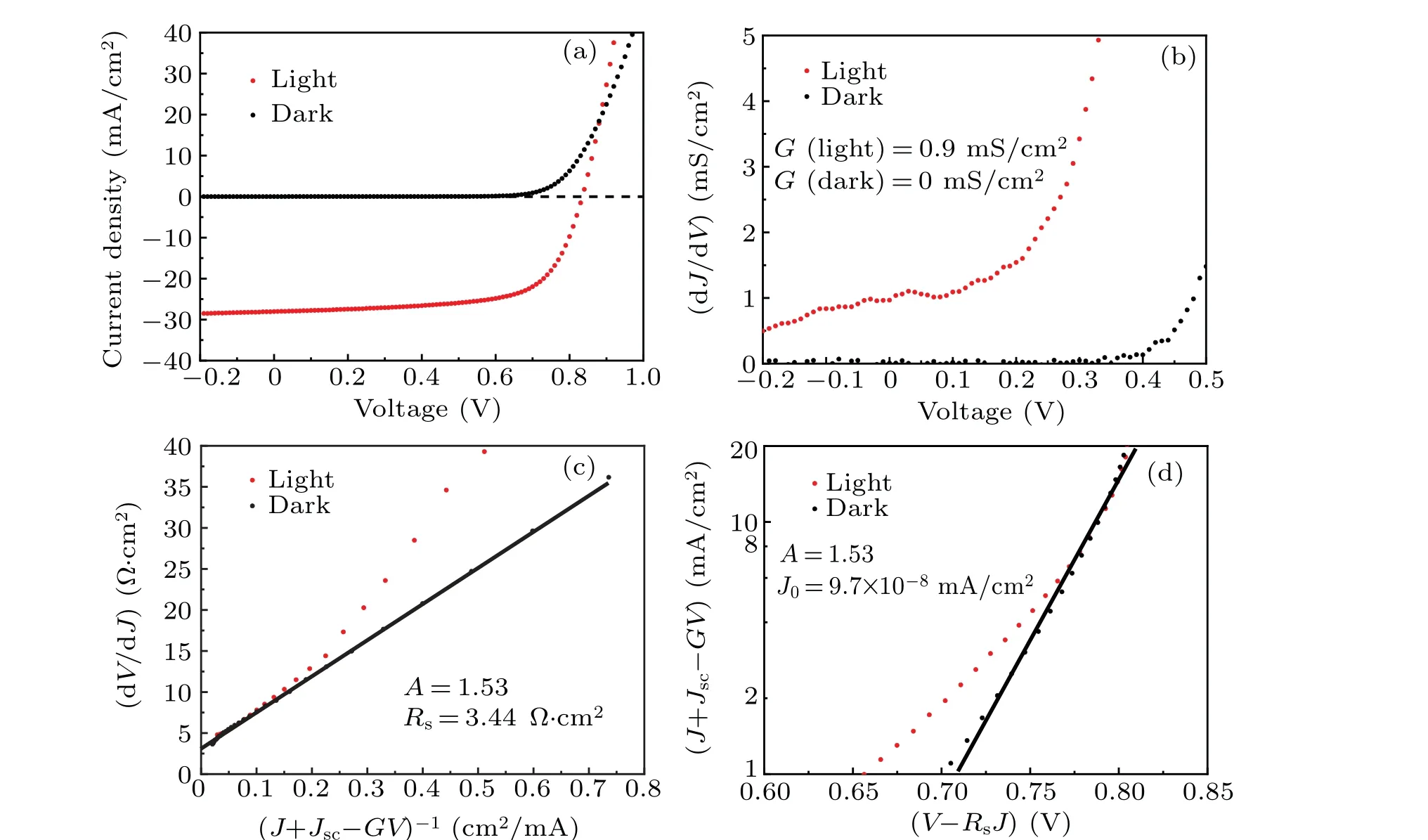
Fig.8. (a)The J–V plots,(b) dJ/dV versus voltage,(c) dV/dJ versus(J+Jsc-GV)-1,and(d)(J+Jsc-GV)versus(V-RsJ),for light(red line)and dark(black line)case.
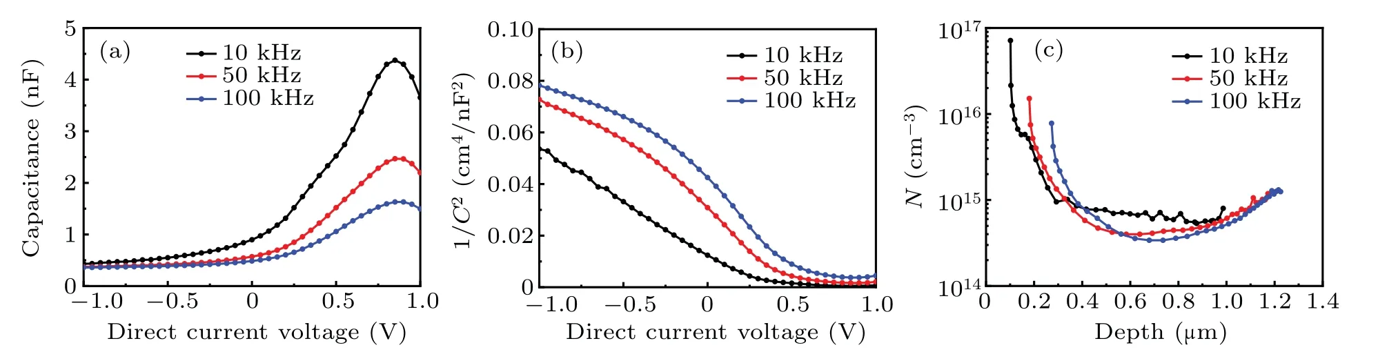
Fig.9. (a)The C–V plots,(b)1/C2–V plots,and(c)space charge distribution,for different frequencies: 10 kHz(black line),50 kHz(red line),and 100 kHz(blue line).
Figure 9(b) shows the plot ofC-2againstV. Under the 10-kHz measurement condition,the data for CdTe device have a line from which the slope and intercept are used to calculate the space charge density(6×1014cm-3)and diffusion voltage(VD=0.4 V). Under the 50-kHz and 100-kHz measurement conditions,the device has a varying slope,implying a spatially varyingN. The relatively low free carrier value identifies one of the key issues in CdTe solar cell technology, namely, the inability to dope CdTe absorbers to a sufficiently high carrier density. Figure 9(c)indicates the depletion width of device is estimated to be about 900 nm. In addition, the depth profile is U-shaped, presenting a trapped electron density and defect vacancy density, which serve as the leakage paths to reduce the shunt resistance.[9]
4. Conclusions and perspectives
In this work, ZnTe:Cu film (200-nm thick) is sputtered by RF-coupled DC bias voltage system and PDHT, to have the carrier concentration of 9.2×1020cm-3and the doping efficiency of 60.9%. After optimizing ZnTe:Cu films, a systematic study is carried out to incorporate ZnTe:Cu film into CdTe solar cell. Optimized band alignment is supposed to enhance the device performance. However, the device with as-deposited ZnTe:Cu contact material shows low current collection and efficiency. The best efficiency of novel device with optimal PDHT for ZnTe:Cu contact material is 15.94%,with correspondingVoc=834 mV,Jsc=27.98 mA/cm2, andFF=68.30%. In general,the improvement of device performance can be attributed to barrier reduction and the suppressed leakage of electricity. The further analysis ofJ–Vbehavior shows that the results of diode ideality factor (A=1.53) between 1 and 2 indicate that the device operates by dominant recombination of trap states in space charge region. TheC–Vprofiling shows that the space charge density remains at 1014level in a frequency range of 10 kHz–100 kHz. Furthermore,the depletion width can be estimated at 900 nm. With all the analysis considered,it is recommended that CdTe-based solar cells be constructed with a ZnTe:Cu back contact layer with optimizing RTP treatment, thereby improving the device performance.
Acknowledgements
The authors are grateful to the Photovoltaic Laboratory at Colorado State University for the CurVA 2.0 software.
Project supported by the Research Foundation of Institute of Electrical Engineering,Chinese Academy of Sciences,(Grant No. Y710411CSB), the Lujiaxi International Team Project of Chinese Academy of Sciences (Grant No. GJTD-2018-05),the Chinese Academy of Sciences President’s International Fellowship Initiative(Grant No.2020VEC0008),and the Fund from the Institute of Electrical Engineering and Advanced Electromagnetic Drive Technology,Qilu Zhongke.
- Chinese Physics B的其它文章
- Design of vertical diamond Schottky barrier diode with junction terminal extension structure by using the n-Ga2O3/p-diamond heterojunction
- Multiple modes of perpendicular magnetization switching scheme in single spin–orbit torque device
- Evolution of the high-field-side radiation belts during the neon seeding plasma discharge in EAST tokamak
- Phase-matched second-harmonic generation in hybrid polymer-LN waveguides
- Circular dichroism spectra of α-lactose molecular measured by terahertz time-domain spectroscopy
- Recombination-induced voltage-dependent photocurrent collection loss in CdTe thin film solar cell