
Graphene-based heterojunction for enhanced photodetectors
2022-03-12 07:49:56HaitingYao姚海婷XinGuo郭鑫AidaBao鮑愛達(dá)HaiyangMao毛海央YouchunMa馬游春andXuechaoLi李學(xué)超
Chinese Physics B 2022年3期
關(guān)鍵詞:游春
Haiting Yao(姚海婷) Xin Guo(郭鑫) Aida Bao(鮑愛達(dá)) Haiyang Mao(毛海央)Youchun Ma(馬游春) and Xuechao Li(李學(xué)超)
1National Key Laboratory for Electronic Measurement Technology,North University of China,Taiyuan 030051,China
2Institute of Microelectronics of Chinese Academy of Sciences,Beijing 100029,China
Keywords: graphene-based heterojunction photodetector, photocurrent generation mechanism, classification of graphene-based heterojunction, graphene-transition metal dichalcogenide (TMD) heterojunction
1. Introduction
Graphene has attracted extensive attention in the field of optoelectronic detection since its discovery in 2004,[1]due to its excellent physical and chemical characteristics. For example, single-layer graphene as an electrode has ultra-high optical transparency (reaches up to 97.7%) and excellent conductivity,which increases the effective receiving area and enhances the carrier collection of the detector compared with traditional metal;[2]and graphene as the contact layer is conductive to generating strong photocurrent at the contact interface as a result of the internal (built-in) electric field.[3,4]The unique zero bandgap structure of graphene makes it theoretically absorb incident light at any wavelength;[5]and its prominently high carrier mobility is beneficial for the realization of the ultrafast response of graphene photodetectors.[6]However, the light absorption of single-layer graphene in the ultraviolet(UV)to near-infrared(NIR)region is extremely low(only 2.3%),resulting in a shorter light-matter interaction,and limiting the application of light harvesting.[7-9]Besides, the ultra-fast carrier recombination speed, ultra-short carrier lifetime, and large dark current of graphene photodetectors are also unsatisfactory to the requirements of the high response current.[10,11]
To resolve the impact of graphene defects on the performance of graphene photodetectors,there are two methods: (i)changing the band structure of graphene to produce a limited band gap, and (ii) combining with a narrow bandgap semiconductor to form a heterojunction.[12,13]Deanet al.[14]first demonstrated in 2010 that the properties of graphene heterojunctions were not only dependent on the material properties,but were also affected by the heterostructure.Since then,many types of graphene-based heterojunctions have been proposed,mainly including the Schottky heterojunction,the type-II heterojunction, the Z-scheme heterojunction, the van der Waals(vdW)heterojunction,the inplane heterojunction and the multicomponent heterojunction.[15]The Schottky heterojunction can effectively separate the photogenerated carriers through the potential barrier and reduce their recombination. Type-II heterojunctions include n-n junctions, p-n junctions, surface heterojunctions and phase junctions,which are also beneficial for the separation of photogenerated carriers.[16]The vdW heterostructure,with a smooth interface and undangling bonds,exhibits surprising physical properties,[17,18]where the atoms in each layer (in-plane) of the material are bound together by covalent bonds and the atomic layers without dangling bonds (out-of-plane) are combined through the weak vdW interactions.[19-21]Particularly, the vdW heterojunction can effectively modulate the material bandgap and reduce charge trapping or scattering in the heterojunction, thus realizing the transport of ultra-fast carriers.[22-24]Currently,many vdW materials can be used,such as black phosphorus(BP),[25]transition metal dichalcogenides(TMDs)(molybdenum disulfide (MoS2),[26,27]tungsten disulfide (WS2), topological insulator materials (Bi2Te3), and compound materials formed by group V and group III (gallium arsenide (GaAs)).[28,29]The novel performance of the heterojunction greatly expands the application range of the material, and provides infinite possibilities to create optoelectronic devices with excellent performances.[30-33]
In this paper, we review graphene-based heterojunctions for enhancing the performance of optoelectronic devices, especially photodetectors. Firstly, the preparation methods and basic parameters of graphene-based heterojunction photodetectors are introduced, and the performance of graphenebased photodetectors prepared using different methods in the last five years are summarized. Secondly, we focus on the photoelectric conversion mechanism,especially the photocurrent generation mechanism, including photovoltaic, photoconductive and photogating effects. Thirdly, the classification of graphene-based heterostructures in different directions is introduced. Meanwhile, the latest research progress of graphene/TMD photodetectors using TMDs (MoS2, WS2) to form heterojunctions is emphasized. Finally,the current challenges of graphene-based photodetectors are summarized,and further prospects are proposed.
2. Preparation and basic parameters for graphene-based photodetectors
2.1. The preparation methods of graphene-based photodetectors
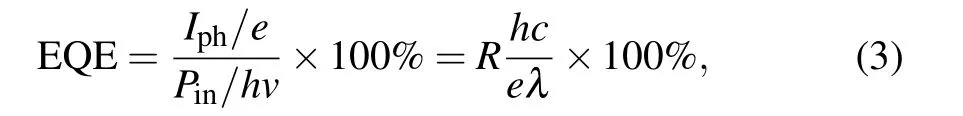
The fabrication of a heterojunction is the key to the development and application of heterojunction optoelectronic devices.Compared with a graphene photodetector,the graphenebased heterojunction photodetector possesses additional advantages by combining graphene with thin-layer semiconductor nanomaterials and undergoing a series of processes.For example, Niet al.[34]designed a graphene-based hybrid phototransistor using plasmonic boron-doped silicon quantum dots, which enhanced the mid-infrared absorption of graphene,and the electron-transition-based optical absorption of boron-doped silicon quantum dots in the ultraviolet to nearinfrared region led to photogating in graphene. The device showed an ultrahigh responsivity of~109A·W-1,as shown in Figs.1(a)-1(c). Chenet al.[3]fabricated a BP/MoS2/graphene vdW heterostructure photodetector with detectivity of 2.3×10¹⁰Jones in the mid-wavelength infrared region under blackbody radiation(Figs.1(d)and 1(e)). Miaoet al.[4]reported a vertically stacked graphene-based infrared photodetector using InAs nanowire (NW). Compared with the single InAs NW infrared photodetector, theIlight/Idarkratios of the InAs NW-graphene photodetector were up to 5×10², as shown in Figs.1(f)-1(h). As the most important step in the manufacture of photodetectors, the fabrication process of the heterojunction is emphatically introduced. There are two main methods used to synthesize graphene heterojunctions: artificial stacking and direct growth.[35]The performance of graphene-based heterojunction optoelectronic devices fabricated using different methods in the last five years is listed in Table 1.
The artificial stacking method is the most common method used for preparing arbitrary oriented heterostructures,which assembles individual flakes prepared using micromechanical exfoliation. Georgiouet al.[59]prepared heterostructures by dry transfer. The graphene (bottom contact) was placed on hBN and covered by a thin WS2flake, where WS2acted as an atomic thin barrier between two graphene layers grown by mechanical exfoliation or chemical vapor deposition. An unprecedented current modulation exceeding 1×10⁶at room temperature and a very high on current was allowed through a combination of tunnelling (under the barrier) and thermionic (over the barrier) transport, which fully proved the successful preparation of the graphene/WS2heterostructure. However, some residues and defects caused by the manual transfer on the interface of the material and heterostructure will affect the quality of the heterojunction, and will have a great impact on the performance of the heterojunction photodetector. Direct growth can effectively avoid the contamination of the heterostructure by the transfer process,and the heterojunction can be obtained using a one-step or two-step chemical or physical vapor deposition (CVD/PVD)method. Qiaoet al.[60]used CVD to epitaxially grow Bi2Te3nanocrystals on single-layer graphene to form a heterojunction. Bi2Te3had a lattice mismatch of 2.7% (0.125 °A) with graphene, which was regarded as an ideal material for vdW epitaxial growth.[61,62]Compared with a pristine graphene photodetector, the graphene/Bi2Te3heterojunction photodetector had higher photoresponsivity with 35 A·W-1at 532 nm wavelength and higher photoconductive gain (up to 83). In 2019, Alamriet al.[63]employed a novel method to manufacture graphene/perovskite/graphene(GPG)heterostructures through fully inkjet-printed. And the GPG photodetector exhibited a high responsivity of 0.53 A·W-1. The direct growth method of preparing heterojunctions has been used in the preparation of optoelectronic devices,and the devices present excellent performances. Moreover, there is a huge challenge induced by the lattice incompatibility of nanomaterials for the direct growth method.
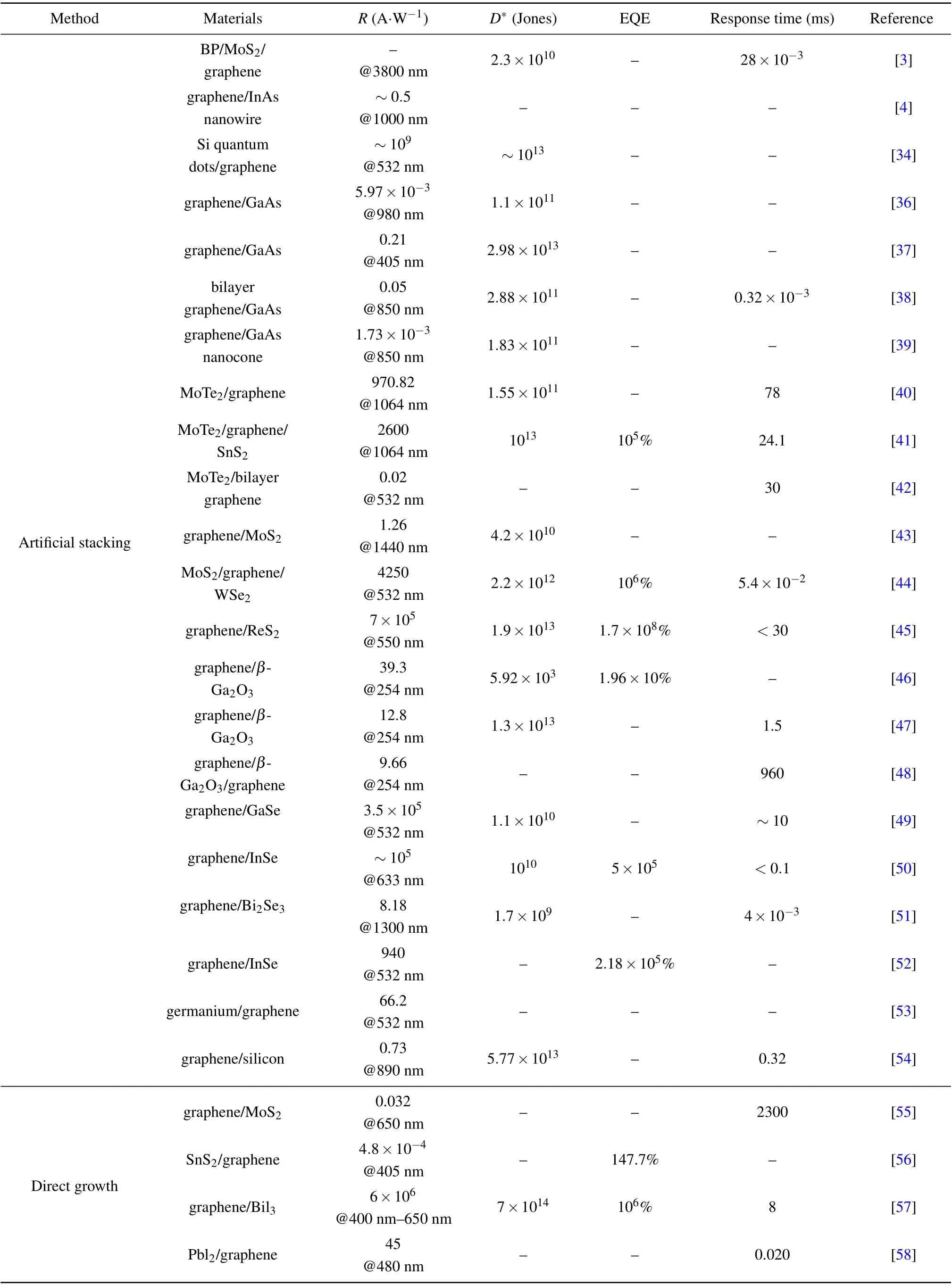
Table 1. The performance of graphene-based heterojunction photodetectors fabricated using artificial stacking and the direct growth method.
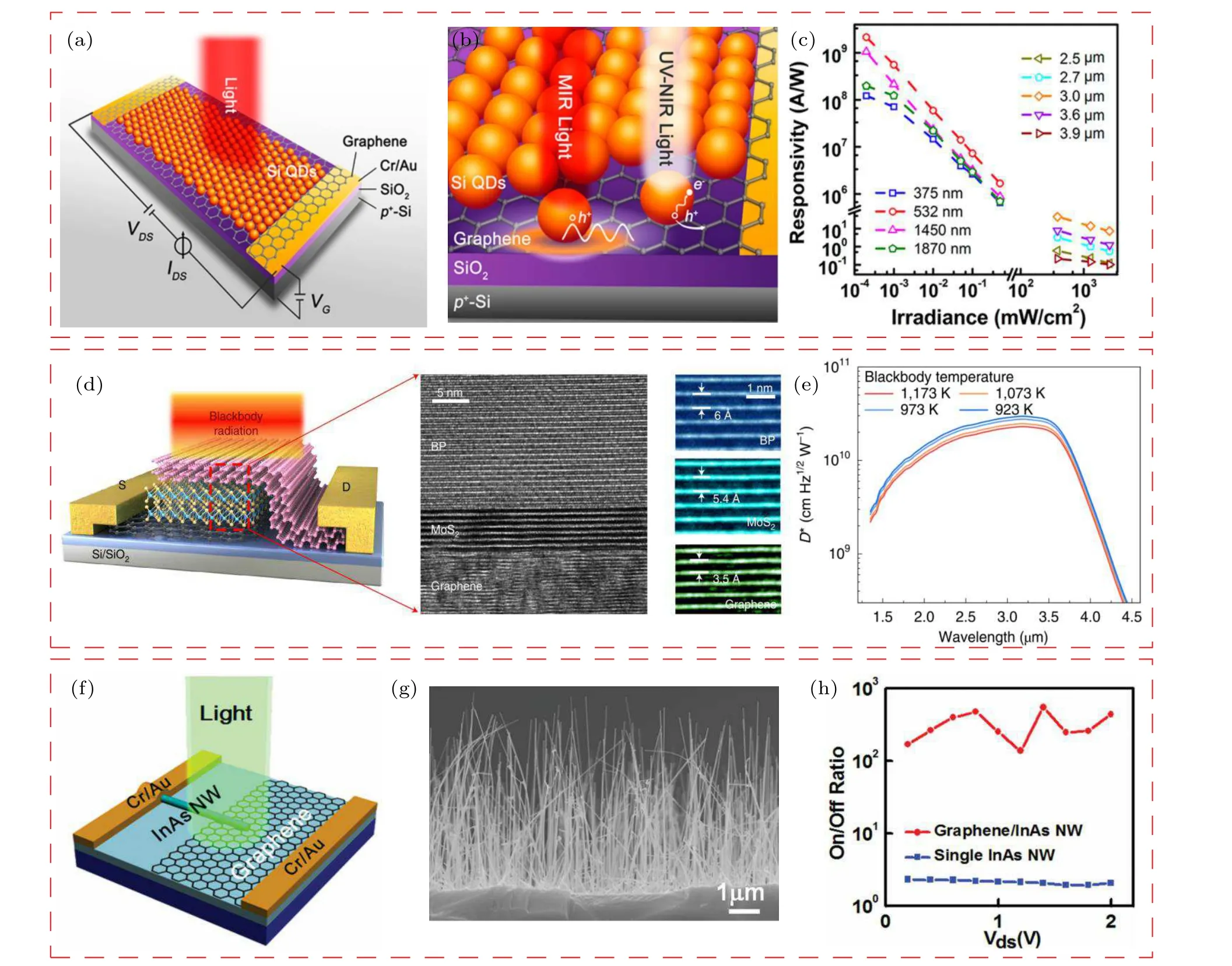
Fig.1. (a),(b)Schematic diagrams of the structure of the hybrid phototransistor. (c)Responsivity of laser irradiance at different laser wavelengths at VG=0 V and VDS=1 V.(d)A schematic diagram of the BP/MoS2/graphene vdW photodetector. (e)D* of the device as a function of the wavelength.(f)A schematic of graphene/InAs NW heterojunction photodetectors. (g)An SEM image of InAs NWs. (h)Ilight/Idark ratios of the graphene/InAs NW and single InAs NW photodetector.
2.2. Basic parameters

Responsivity (R) TheRvalue is calculated by the ratio of the photocurrent or photovoltage to the incident power density,and the formula can be written as wherecis the light velocity,λis the excitation wavelength,andηis quantum efficiency. Gain characterizes the enhancement ability of the external circuit current under the illumination.
Quantum efficiency There are two measures of quantum efficiency: internal and external. External quantum efficiency(EQE) is the ratio of the number of incident photons to the number of electron-hole pairs producing a photocurrent and is given as a percentage. The EQE value is calculated using the following equation:
whereh,v,andcare Planck’s constant,the frequency of incident light and light speed,respectively. The large EQE can be achieved by increasing theRvalue. The internal quantum efficiency(IQE)is the ratio of the number of absorbed photons to collected charge and is given as a percentage. The EQE is usually lower than the IQE, and accounts for the number of photons that the IQE is calculated using actually absorbed photons,while the EQE assumes that all incident photons are absorbed. Losses in generated charge is the charge recombination,both in the bulk and at material interfaces. Therefore,the charge recombination needs to be taken into account in graphene-based vdW heterostructure photodetectors.
Specific detectivity(D*)The detectivityD*is an effective parameter used to evaluate and compare the performance of photodetectors with different materials and geometries. A highD*means a stronger ability to detect weak signals, and theD*can be given by
whereAis the effective area of the photodetectors,Bis the electrical bandwidth,and NEP(noise equivalent power)is defined as the optical power that yields a single signal-to-noise ratio for a given bandwidth and it can be calculated using NEP =In/R. Then,Inandeare the dark current and elementary charge,respectively. It is expressed in units of Jones(cm·Hz1/2·W-1).
Response time(τ)The response time reflects the speed of the detector as it follows the signal changes.The response time is divided into the rise time(τr)and fall time(τf).The response time(τr/τf)represents the required time that the photocurrent rise(fall)from 10%(90%)to 90%(10%)of the entire current.
3. Photocurrent generation mechanism of the graphene-based heterostructure

Fig.2. PN junction under illumination. (a)Separation and movement of photogenerated carriers. (b)A band diagram.
The photocurrent is an important characteristic parameter of photoelectric devices, and the photocurrent generation mechanism can be written as: the semiconductor material absorbs light energy during light irradiation on the graphenebased heterojunction, depending onhv >Eg(h= Planck’s constant andv=photon frequency). It is possible to make electrons transition from the valence band to the conduction band to produce electron-hole pairs,and then generate a photocurrent through movement of additional carriers. An effective photoelectric energy conversion requires three basic elements: (I) the energy absorbed by light exceeds the semiconductor bandgap, resulting in the generation of photogenerated carriers; (II) the carrier diffuses in the semiconductor and reaches an energy barrier,allowing one carrier to pass but blocking the other carrier;(III)the separated carriers move to an external circuit through the semiconductor.[64]There are two mechanisms for generating a photocurrent: photoelectric conversion(including photovoltaic,photoconduction,and photogating) and the thermal effect (including photothermoelectric and bolometric).[65]Here, the photoelectric conversion mechanism is mainly discussed.
The photovoltaic effect relies on the self-built electric field in the space charge region to separate the electron-hole.As soon as the photon penetrates into the space charge, the generated electron-hole pairs are separated immediately by the self-built electric field,and the photo-induced carriers are swept towards N and P, respectively, to form a current, as shown in Fig. 2(a). The holes are toward P and electrons are toward N,and they accumulate gradually,forming the electrical potential difference(Vp)opposite the built-in electric field,andVpis called the photovoltaic effect,as shown in Fig.2(b).To obtain a low dark current and high quantum efficiency,reverse bias or zero bias operation is usually adopted.[66]The photoconduction effect is a phenomenon where the variable illumination induces the conductometric change of semiconductor materials,in which the separation of electron-hole pairs is realized by an external voltage. The working mechanism of the photogating effect is as follows: when the electron-hole pair is generated,one type of carrier is transferred to graphene,and the opposite type of carrier is trapped in the semiconductor. Carriers are trapped at defect interfaces. The Fermi level of graphene is effectively modulated by capacitive coupling,which promotes the delay recombination of carriers and leads to high gain. In addition,the transferred free carriers circulate in the graphene channel several times during its lifetime,thus improving the photosensitivity of the detector.[67-71]
The photogating effect is a promising approach which improves absorption efficiency and produces high responsivity. The traditional graphene/silicon hybrid photodetectors mostly depend on the Schottky barrier of the graphene-silicon interface due to the mismatch of Fermi levels, with only responsivity of hundreds mA·W-1and response time of ms.[72,73]Lightly p-doped Si substrate has been applied in graphene-based photodetectors.[74]Luoet al.[75]generated a built-in electric field at the SiO2/Si interface using a heavily n-doped Si/SiO2substrate,which can separate the photon-induced electron-hole pairs in Si,as shown in Figs.3(a)-3(c). The accumulation of hole at the Si/SiO2interface acted as an additional gate voltage,resulting in the horizontal shift in the transmission curve. Then, it made the significant photoresponsivity in graphene about 500 A·W-1or 4 A·W-1at 450 nm or 1064 nm light, respectively. It provided great potential for ultra-fast graphene photodetectors due to the highspeed separation of the photoninduced electron-hole pairs at the SiO2/Si interface. Fukushimaet al.[76]used photosensitive material (InSb) to inject photocarriers into graphene to change the carrier density on the surface graphene (Fig. 3(d)), and the photogating effect was used to change the carrier density on the graphene surface by modulating the gate voltage of the graphene channel, resulting in high responsivity and low dark current. The photogating voltage and field effect mobility were also evaluated in Figs.3(e)-(f),and the photo response increased to 18.8 times compared to that without the photogating effect.In 2020,Fukushimaet al.[77]initially prepared the p-type InSb substrate with a tetraethyl orthosilicate(TEOS)layer to produce a graphene-based photodetector,as shown in Fig.3(g). When the graphene channel size was reduced from 100 μm2to 25 μm2,the responsivity was improved from 61.7 A·W-1to 321.0 A·W-1(Figs.3(h)-3(i)).
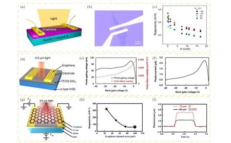
Fig.3. (a)A schematic illustration of a graphene/heavily n-doped silicon photodetector. (b)An optical microscopic image of a typical graphene device.(c)The plot of the calculated responsivity as a function of laser power at various Vbg. (d)A schematic diagram of the InSb-based graphene field effect transistor. (e)Photogating voltage and FE mobility values as functions of negative Vbg. (f)Iph calculated based on the photogating voltage and the FE mobility data. (g) A schematic illustration of a graphene/TEOS/InSb photodetector. (h) The responsivity of devices with different graphene channel areas,and(i)the photocurrent-time plot for devices with 100 μm2 (black solid line)and 25 μm2 (red dotted line)graphene channel areas.
4. Typical graphene-vdW heterostructure and photodetectors
4.1. The classification of the graphene-vdW heterostructure
Since the 2D materials are connected through van der Waals interactions, the graphene-based heterojunctions are constructed by superimposing with sublayers in any direction.[19]According to the arrangement and relative position of graphene with other materials,the heterojunction can be divided into two kinds of structures: lateral and vertical heterostructures.[78]The energy band structure of the heterojunction interface promotes the formation, drift and recombination of photogenerated carriers and further strengthens the photoelectric performance of the graphene heterojunction photodetector.[79,80]
4.1.1. Vertically stacked graphene-based heterostructure
One material is stacked on the top of the other to form a vertical heterojunction through vdW force,and the structure of the heterojunction actually refers to the entire contact plane.The vertical heterojunction was usually synthesized using epitaxy or mechanical exfoliation.[81]In particular,the mechanical exfoliation method can generally only be used to develop vertical heterostructures. Compared with the laterally stacked heterojunction,the vertically stacked heterostructure provides a larger surface area for the interface layered material and involves a tunneling effect between two layers, which is very suitable for photosensitive device applications.[82]
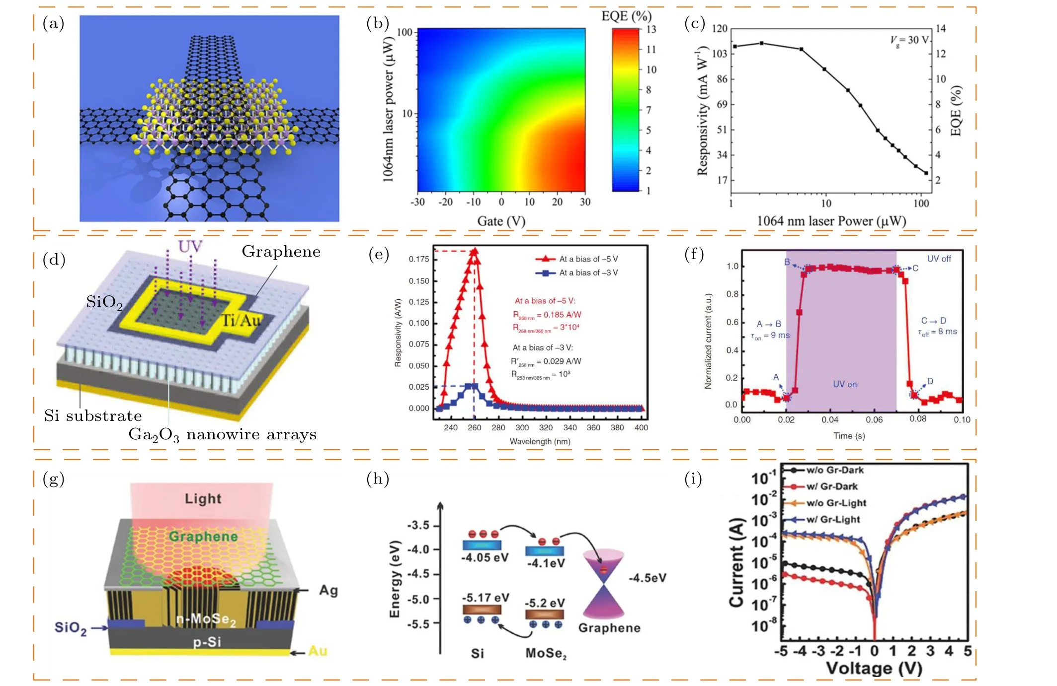
Fig.4. (a)A schematic diagram of the graphene-MoTe2-graphene vdW heterostructure. (b)Near infrared light response performance. The dependence of EQE on back-gate voltage and incident laser power. (c) The relationship between the optical responsivity and EQE of the device and the incident optical power.(d)A schematic diagram of the device.(e)The spectral response of PDs based on the graphene/vertical Ga2O3 nanowire array heterojunction. (f)The normalized response on a linear scale. (g)A schematic illustration of the graphene/MoSe2/Si heterojunction photodetector with a graphene transparent electrode. (h) Energy band alignments of the MoSe2/Si heterojunctions with a graphene transparent electrode. (i) Typical I-V curves of the MoSe2/Si heterojunction with and without a graphene transparent electrode measured in dark and under white light illumination (23 mW·cm-2),respectively.
Many vertically stacked heterostructures involving the quantum tunneling effect were proposed.[83,84]For example,Bala Kumaret al.[84]proposed a vertical tunneling field-effect transistor (FET) based on graphene heterojunctions with layers of hBN. Here, the graphene worked as the contact layer,the hBN or MoS2was usually sandwiched between graphene layers, and the fieldeffect transistor functions were based on quantum tunneling across the thin layer of insulation channel barrier(hBN or MoS2). Britnellet al.[85]studied carrier tunneling in graphene heterostructures,in which boron nitride or molybdenum disulfide acted as a vertical transmission barrier.The graphene electrode could be controlled by applying the voltage to the silicon substrate.Zhanget al.[86]designed a vertical graphene-MoTe2-graphene vdW heterostructure using a set-controllable transfer method (Fig. 4(a)). Because of the high absorption coefficient of MoTe2, the device performed a uniform photoresponsive area. The device can operate in visible and NIR light under self-powered conditions due to photogenerated carriers obtained by a built-in electric field at zero bias voltage. Moreover,the photosensitivity and EQE of the photodetector were modulated by controlling the back gate voltage. When the incident light power was fixed,the EQE increased with the increase in the back gate voltage,as shown in Fig.4(b).WhenVgwas 30 V,the optical responsivity and EQE first remained constant, and then decreased monotonously with the incident light power(Fig.4(c)). Experimental results showed that when the 1064 nm incident light power was less than 5 μW,a high photoresponsivity(110 mA·W-1),high external quantum efficiency (EQE: 12.9%), and high speed (a rise time of 24 μs and a fall time of 46 μs) were obtained,indicating the essential role of two Schottky barriers between graphene and MoTe2for photocurrent generation. And in the NIR range, the performance of this device was higher than other reported photodetectors based on layered semiconductors. Heet al.[87]prepared Ga2O3nanowires by thermally oxidizing GaN nanowires and using a molecular beam epitaxy technique on an n-doped Si substrate (Fig. 4(d)). Compared with Ga2O3films,more carriers were generated in vertical Ga2O3nanowire arrays. The graphene was transferred to the Ga2O3nanowire and acted as a transparent electrode,and then a graphene/vertical Ga2O3nanowire array photodetector was formed. This heterojunction photodetector showed high solar-blind UV performance, as shown in Figs.4(e)and 4(f). Responsivity was 0.185 A·W-1, and the rise and fall time were 9 ms and 8 ms, respectively. Maoet al.[88]prepared a photodetector with a high-speed broadband response.Graphene acted as a transparent electrode and a p-type Si substrate was combined with n-type MoSe2film to complete the preparation of the MoSe2/Si heterojunction, as shown in Fig. 4(g). Under light irradiation, the electron was injected into the MoSe2film, while the hole was injected into the ntype Si to form a photocurrent. The structural band diagram is shown in Fig.4(h). Figure 4(i)depicts the current and voltage(I-V)characteristics of the heterojunction. With the graphene transparent electrode, the dark current in the reverse bias direction (-5 V) and forward bias direction (+5 V) decreased and increased, respectively. Accordingly, the graphene rectification rate in the range of±5 V was significantly improved.Under light illumination,the photocurrent of-5 V increased.The high electrical conductivity of graphene was helpful in improving the photocurrent of MoSe2/Si devices. Except for the vertical tunneling field-effect transistor and the gate/voltagecontrolled tunneling photodetector mentioned above, the resonant tunnelling is another quantum tunnelling system in the vertically stacked heterostructure.[89,90]For example, Linet al.[89]presented the direct synthesis of MoS2/WSe2/graphene and WSe2/MoS2/graphene heterostructuresex situusing oxide powder vaporization and metal-organic chemical vapor deposition(MOCVD)methods. The direct grown heterostructures exhibited resonant tunnelling of charge carriers, which led to sharp negative differential resistance at room temperature. And the peak of the resonant tunnelling could be tuned by modifying the stacking order or layer composition, which could have potential applications in ultra-low-power electronic and photodetector devices.
4.1.2. Laterally stacked graphene-based heterostructure
A lateral heterojunction refers to the fact that two materials are located in the same plane, and the atoms of the two materials are usually connected together by covalent bonds to form a line or a ribbon at the interface,accompanied by the appearance of some specific physical properties at the interface.In addition,the quality of the epitaxy is positively promised in the lateral heterojunction,and essentially reinforces the optical and electrical performance of the device.
The combination of graphene and a two-dimensional semiconductor can significantly affect the position of the Fermi level of graphene by the superposition method, and it is possible to construct an internal p-n junction in graphene.Menget al.[91]reported the preparation of a lateral graphene p-n junction based on a graphene/MoS2mixed interface.MoS2transferred light-generated carriers to graphene, and the graphene p-n junction demonstrated obvious photocurrent generation. Thus, the optical response of the device was improved. In 2019,WS2was directly synthesized in the prepatterned graphene gaps on silicon wafers using a hydrogenassisted CVD growth process by Chenet al.,[92]as shown in Fig. 5(a). Herein, the WS2was applied as the channel material of an n-type field-effect transistor (FET). And the lateral graphene/WS2/graphene heterojunction showed a high responsivity of 121 A·W-1at the wavelength of 532 nm and the illuminance of 2.7×10⁵mW·cm-2(Figs. 5(b) and 5(c)),which was about 2 orders of magnitude more than similar devices manufactured in layers. It was indicated that the method provides the possibility for scalable manufacturing of high-quality 2D lateral electronic and optoelectronic devices. In the same year, Liuet al.[93]prepared a lateral graphene/MoS2/graphene heterostructure photodetector,shown in Fig. 5(d). The graphene film was grown and patterned into two stripes using a plasma etching process, and MoS2film was synthesized in the spacing section (15 mm)between the two stripes using CVD. Figure 5(e) exhibits the corresponding energy band diagram; the barrier heightqφ1was greater thanqφ2in the device resulting from growth. It was also demonstrated that the formed Schottky junction between graphene and MoS2was a key part of the photoelectric response,where the MoS2spontaneously generated lightexcited electron-hole pairs and separated quickly,resulting in the fast transfer of electron to graphene. In contrast,the transferred electron from graphene to MoS2needed an applied electric field to suppress the Schottky barrier. The higher the applied electric field, the lower the barrier height, resulting in bigger current density. Therefore,the tunable Schottky barrier can be obtained by adjusting the applied voltage, and then it suppressed the dark current in the graphene-MoS2interface.As shown in Fig.5(f),in the case ofVg=0 V,a significantly stronger response appeared during 450 nm-680 nm. The responsivity of the device was greater than 2×10³mA·W-1,and the maximum specific detectivityD*was as high as 1013Jones. Chenet al.[94]designed a graphene/GaS/graphene lateral heterojunction (Fig. 5(g)). First, graphene was grown by CVD and transferred onto the Si substrate, and electron beam lithography was performed to form a graphene electrode pair. Then,the GaS was selectively deposited in the graphene gaps, and the graphene/GaS/graphene lateral heterojunction was formed. Under excitation of light with a wavelength of 270 nm,the photosensitivity was as high as 11.7 A·W-1,and the detection limit could be reduced to 2.61 μW·cm-2, as shown in Fig. 5(h). Figure 5(i) illustrates that the response time was less than 60 ms,which made the device a promising application in fast photo-switching.

Fig. 5. (a) A schematic illustration of Gr:WS2:Gr FET. As-calculated photoresponsivity under (b) 0 V and (c) 30 V gate voltage. (d) A schematic diagram of the heterostructure. (e) A band diagram of two opposing Schottky junctions connected in series. (f) The responsivity R (black curve)and specific detectivity D* (red curve) with a wavelength of 450 nm to 700 nm at Vg =0 V. (g) A schematic of the graphene/GaS/graphene lateral heterojunction photodetector. (h) The calculated photoresponsivity-Vds plot at different incident power. (i) One typical on-off switching current vs.time plot in the response time measurement.
4.2. Typical graphene/TMDs vdWs heterostructure for photodetectors
Generally,the optical absorption and response properties of graphene can be improved by tuning the graphene bandgap using electrostatical or chemical methods, but is always accompanied by the reduction of ultrafast carrier mobility and other specific properties. Therefore, we focus on the layered materials (TMDs), which are similar to the graphene structure. The TMD crystal structure is composed of three layers of atoms, where the upper and lower chalcogenide atoms sandwich the transition group atoms to form a“sandwich”XM-X structure.[95]Each layer of TMD material has a hexagonal lattice structure. Although the layers of TMDs are connected by weak van der Waals forces, their structure is very stable. Moreover,TMDs have many excellent properties,such as a large band gap, good light absorption characteristics and strong covalent bonds, etc., which form a complementary relationship with graphene.[96]The typically represented TMDs(MoS2and WS2)are discussed as follows.
MoS2is a tightly packed hexagonal layered structure.Generally,the MoS2crystal is a semiconductor material with an indirect band gap of 1.2 eV.[97]However, when the thickness of MoS2is reduced to one layer,it converts into a direct band gap(1.90 eV)semiconductor material.[98]As the number of MoS2layers gradually increases,the bandgap decreases.[99]Moreover, multilayer MoS2offers a wider spectral response from ultraviolet(UV)to near infrared(NIR)wavelengths due to its narrower bandgap, which is advantageous in a variety of photodetector applications.[100,101]Due to the excellent electric charge transport characteristics of graphene and the high absorption coefficient of MoS2in the visible light, the MoS2/graphene heterostructure photodetector was used as a working electrode in the photoelectrochemical (PEC)-type photodetector.[102]In 2016, Fazioet al.[103]prepared a flexible graphene/MoS2heterostructure photodetector. As shown in Fig. 6(a), the heterostructure was fabricated by stacking graphene on top of MoS2. In this device,the MoS2layer acted as a visible light absorber, graphene was used as a photocurrent transmission channel,and MoS2injected the light-excited electrons into the graphene channel. The operation principle of the device is depicted in Fig.6(d). Since the transparency of polyethylene terephthalate (PET) in the visible light was~90%, PET with high transparency and good flexibility was selected as the flexible substrate. The device retained~82% light transmittance (Fig. 6(b)). At the wavelength of 642 nm,the device exhibited an internal photoresponsivity of 570 A·W-1and an external photoresponsivity of 45.5 A·W-1(Fig.6(c)),which was at least two orders of magnitude higher than the bulk semiconductor flexible film. And the photoconductive gain was as high as 4×10⁵. This flexible photodetection was expected in wearable applications. Hossainet al.[104]constructed a biocompatible heterostructure photodetector using photo-active MoS2and highly conductive graphene. It facilitated the charge collection of the photocarriers and was photoresponsive to broadband incident radiation in the visible light system. The photoresponsivity of the device was~0.30 A·W-1(103times higher than other reported devices),and the detectivity was up to~3.6×10¹⁰Jones.[105,106]To further enhance the performance of graphene/MoS2heterostructure photodetectors, high-quality MoS2and graphene with fewer defects are needed. In 2018, a continuous singlelayer MoS2film of several square millimeters was grown using CVD by Sunet al.[107]The MoS2and graphene films were transferred onto PET substrates sequentially, forming a vertically stacked MoS2/graphene heterojunction photodetector (Fig. 6(e)). The external photoresponsivity was 3.5 A·W-1, when the incident power was 60 μW at a wavelength of 520 nm,Vgs=-1 V andVds=1 V, as illustrated in Figs. 6(f) and 6(g). In particular, the internal photoresponsivity was up to 33.3 A·W-1, which was higher than most flexible photodetector devices. The Schottky barrier is another key factor that affects optoelectronic devices. The optoelectronic device performance can be enhanced by adjusting the height of the Schottky barrier. In 2019,Leeet al.[108]designed a graphene/MoS2heterojunction fieldeffect transistor. Graphene was used as source, drain and gate materials,a single-layer MoS2sheet was applied as piezoelectric channel material, and a h-BN sheet was utilized as a gate polar insulator. The Fermi level of graphene and the corresponding Schottky barrier were greatly modulated by the strain induced polarization of the MoS2charge. The sensitivity of this device can be improved using a variable Schottky barrier. And then a graphene/MoS2heterojunction phototransistor with a short channel length and adjustable Schottky barrier was proposed to improve the photodetector performance in 2020. Leeet al.[109]prepared a sub-30 nm channel length between the graphene source and drain electrode to reduce carrier loss by recombination and to decrease transit time in MoS2. Meanwhile, the Schottky barrier was controlled by a gate electric field or photoinduced doping. And then the performance of the phototransistor was greatly improved,with responsivity of 2.2×10⁵A·W-1and detectivity of 3.5×10¹³Jones.
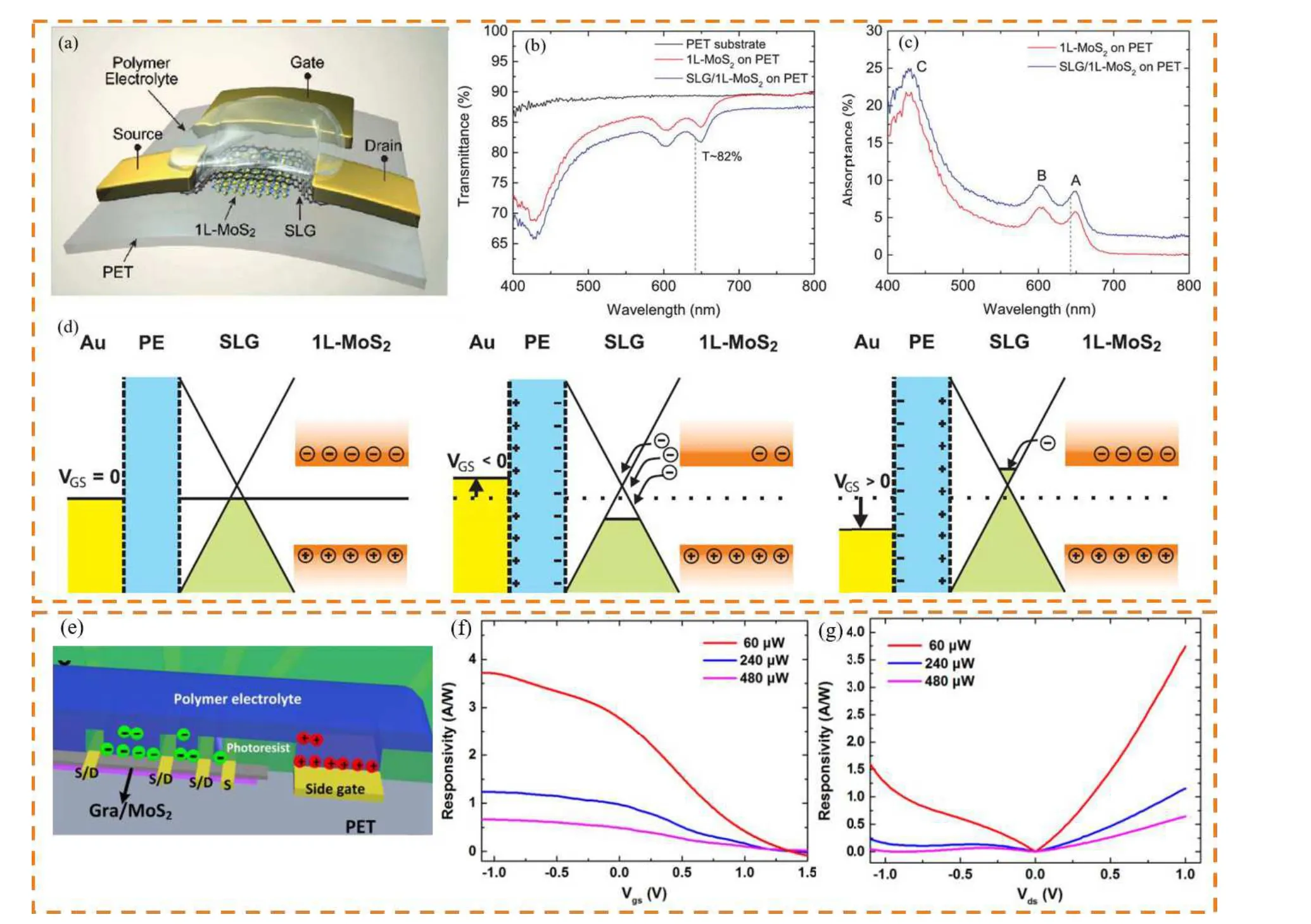
Fig. 6. (a) A schematic illustration of SLG/MoS2 flexible PD. (b) and (c) The transmittance and absorbance of 1L-MoS2 and SLG/1L-MoS2 curves.The dotted line was the test wavelength. (d) A schematic band diagram of PE gated SLG/1L-MoS2 PD at zero, negative, and positive Vgs. (e) The working principle of the side-gated flexible MoS2/graphene heterojunction photodetector. (f)Responsivity as a function of the Vgs and incident power.(g)Responsivity as a function of Vds and incident power.
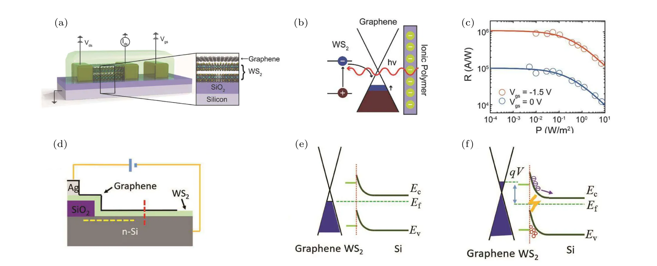
Fig. 7. (a) A schematic diagram of the WS2/graphene heterostructure photodetector structure. (b) A schematic diagram of the charge transfer on the WS2/graphene interface. (c)The relationship curve between incident light power and responsivity. (d)A schematic of the device. The band alignment along the red dashed line in(e)the dark state,and(f)under light illumination with negative bias.
As a typical TMD material,the WS2energy band transition mode can be transformed by changing the layer number;for example,the energy band gap of WS2can be changed from the indirect bandgap 1.3 eV of the crystalline material to the direct bandgap 2.0 eV of the semiconductor.[110]More importantly, the combination of WS2and graphene can modify the shortcomings of the low switching ratio caused by the zero bandgap of graphene. And the WS2/graphene heterostructure photodetector shows excellent photoelectric properties,including a high optical absorption coefficient (105cm-1-106cm-1) and a large exciton binding energy (700 meV-800 meV).[111-113]Moreover, compared with MoS2, WS2has a greater room-temperature phonon-limited electron mobility, which can be widely applied in nano-optoelectronic devices.[114]
In 2016, Tanet al.[115]developed a photodetector with a horizontal graphene-WS2-graphene structure. The singlelayer WS2was used as the active semiconductor in the ultrathin photodetector device. Graphene was used as a 2D electrode, which enabled the photoresponsivity of the device to be modulated by the electrostatic gating and light input control. When the illumination power density was 2.5×10⁷mW·cm-2, the photoresponsivity reached 3.5 A·W-1.A high-response broadband photodetector based on a WS2-graphene heterostructure was reported by Lanet al.[116]The device exhibited a wide spectral response in the range of 340 nm to 680 nm and a maximum responsivity up to 950 A·W-1at a wavelength of 405 nm, due to the excellent broadband absorption capacity of single-layer WS2and the internal built-in electric field at the WS2-graphene interface,which can promote the effective separation of photogenerated electron-hole pairs. In the same year,Mehewet al.[117]successfully fabricated an atomically thin WS2-graphene heterostructure photodetector with an ionic polymer gate(Fig.7(a)).Based on the photogating effect,the WS2layer was used to absorb photons and divided into electron-hole pairs at the interface due to the different work function between graphene and WS2, with one type of carrier transferred to graphene and the rest remaining in WS2(Fig.7(b)). The relationship plot between responsivity and incident optical power are shown in Fig.7(c)whenVgs=0 V andVgs=-1.5 V.WhenVds= 100 mV andVgs=-1.5 V, the responsivity reached 1×10⁶A·W-1: four orders of magnitude higher than traditional graphene-based photodetectors.The detector could conduct at a bandwidth up to 1.5 kHz and maintain an internal gain of 106. Moreover,it showed a detectivity of 3.8×10¹¹Jones,which was close to the responsivity of a single photon counter;and it can be used in a wide band(400 nm-700 nm)for videoframerate imaging applications. Xiaoet al.[118]reported a high-performance photodetector based on a graphene/WS2/Si vdW heterostructure(Fig.7(d)). In the dark,an internal electric field was formed between Si and graphene(Fig.7(e)). Under negative bias and light irradiation,the generated electronhole pairs were separated, and the holes would move toward the graphene and be trapped in the WS2-Si potential well, as shown in Fig. 7(f). The device overcame the shortcomings where non-charge neutrality cannot be compensated due to the interference of electron contact,and performed a high light responsivity response(54.5 A·W-1at 800 nm)and fast response rate(the rise time was 45 μs,fall time was 210 μs).
5. Summary and outlook
Graphene-based heterojunctions have potential applications in future smart devices and wearable and flexible biomedical electronic systems due to their layered material structure and excellent optoelectronic properties. We review typical graphene-based heterojunction photodetectors and two-dimensional vdW nanomaterials as light-absorbing materials, focusing on photocurrent generation mechanisms,including photovoltaics, photoconductivity and photogating. Meanwhile, the classification of graphene-based heterojunctions in different directions is summarized.So far, the performance enhancement of graphene-based photodetectors mainly includes adjustment of the interface of the graphene/semiconductor heterostructure, electrical gating/chemical doping of graphene, surface plasmon enhancement, etc. However, the heterojunction photodetectors based on graphene are still at the initial stage,and the following aspects need to be further explored: (I) the high electrical conductivity of continuous graphene leads to a high dark current and low detection rate, and the performance of the prepared devices needs to be improved. (II) The graphene-based heterojunction preparation method has some defects,such as lattice mismatch and poor interfacial cleanliness of artificially stacked heterojunctions. (III) The large-area growth methods of high-quality layered nanomaterials with low numbers of structural defects are highly desired. Whether the preparation method of graphene vdW heterojunctions is applicable to other material heterojunctions remains to be further discussed.
Acknowledgments
Project supported by the National Natural Science Foundation of China (Grant No. 61771467), Shanxi Scholarship Council of China (Grant No. 2020-112), Scientific and Technological Innovation Programs of Higher Education Institutions in Shanxi, China (Grant Nos. 2020L0268 and 2020L0307), and Science Foundation of North University of China(Grant No.XJJ201915).
猜你喜歡
青年文學(xué)家(2021年16期)2021-08-05 14:18:46
初中生世界(2020年13期)2020-12-17 13:07:31
戲曲研究(2020年2期)2020-11-16 01:21:24
初中生世界·七年級(jí)(2020年4期)2020-04-30 06:47:37
揚(yáng)子江詩(shī)刊(2018年5期)2018-11-13 08:31:49
詩(shī)潮(2018年10期)2018-10-17 06:50:36
未來(lái)英才(2016年5期)2016-05-14 07:01:21
花火B(yǎng)(2016年8期)2016-05-14 03:09:56
讀者欣賞(2014年5期)2014-07-03 03:35:36
讀者欣賞(2014年5期)2014-05-13 15:08:03

- Chinese Physics B的其它文章
- Surface modulation of halide perovskite films for efficient and stable solar cells
- Lithium ion batteries cathode material: V2O5
- A review on 3d transition metal dilute magnetic REIn3 intermetallic compounds
- Charge transfer modification of inverted planar perovskite solar cells by NiOx/Sr:NiOx bilayer hole transport layer
- A low-cost invasive microwave ablation antenna with a directional heating pattern
- A DFT/TD-DFT study of effect of different substituent on ESIPT fluorescence features of 2-(2′-hydroxyphenyl)-4-chloromethylthiazole derivatives