
Ambipolar performance improvement of the C-shaped pocket TFET with dual metal gate and gate-drain underlap
2023-11-02 08:13:36ZiMiaoZhao趙梓淼ZiXinChen陳子馨WeiJingLiu劉偉景NaiYunTang湯乃云JiangNanLiu劉江南XianTingLiu劉先婷XuanLinLi李宣霖XinFuPan潘信甫MinTang唐敏QingHuaLi李清華WeiBai白偉andXiaoDongTang唐曉東
Chinese Physics B 2023年10期
關鍵詞:趙梓
Zi-Miao Zhao(趙梓淼), Zi-Xin Chen(陳子馨), Wei-Jing Liu(劉偉景),?, Nai-Yun Tang(湯乃云),Jiang-Nan Liu(劉江南), Xian-Ting Liu(劉先婷), Xuan-Lin Li(李宣霖), Xin-Fu Pan(潘信甫),Min Tang(唐敏), Qing-Hua Li(李清華), Wei Bai(白偉), and Xiao-Dong Tang(唐曉東)
1College of Electronics and Information Engineering,Shanghai University of Electric Power,Shanghai 200090,China
2Semiconductor Manufacturing International Corporation,Shanghai 201203,China
3Radiwave Technologies Corporation Limited,Shenzhen 518172,China
4Key Laboratory of Polar Materials and Devices,East China Normal University,Shanghai 200041,China
Keywords: tunnel field effect transistor,ambipolar current,dual metal gate,gate-drain underlap
1.Introduction
With Moore’s law, MOSFET devices have scaled to the nanometer size, the number of devices and components on a single chip has increased dramatically, and today we have a significant increase in the ability of data processing.However, to further scale, MOSFETs start to face a series of challenges: short-channel effects (SCEs), hot-carrier effects(HCEs), higher power consumption, etc.To meet these challenges, one of the solutions is to find new devices to replace MOSFETs.The tunneling field-effect transistor (TFET) is one of the promising devices to replace CMOS for low-power applications.[1]The conduction mechanism of TFETs is bandto-band tunneling (BTBT), which is the key phenomenon for the conduction of current in this quintessential reversebiased gated p-i-n structure, unlike MOSFETs, where conduction is due to the transition of charge.[2]With a lower subthreshold swing (SS), TFETs can break the 60 mV/decade limit at room temperature, and achieve lower off-state currents and better immunity to short-channel effects.However,there are still two main problems with TFETs: the low onstate currentIon, and the ambipolar characteristics.To address the low on-state current problem, researchers have now proposed a number of solutions, such as the introduction of heterostructures,including heterogeneous gate dielectrics,[3-5]source channel heterojunctions,[6-8]and heterogeneous gate materials;[9,10]the introduction of line tunneling structures to increase the tunneling area;[11-16]utilization of black phosphorus instead of silicon materials;[17,18]insertion of a metal strip in the gate oxide layer;[19]and the introduction of pocket structures.[20,21]Ambipolar conduction makes the TFET less effective in complementary circuits and restricts its utility in digital circuit design.Several solutions have been proposed to suppress ambipolar currents: using asymmetric doping,[22-24]gate-drain underlap,[23,25,26]gate-drain overlap,[27]heterogeneous dielectrics,[23,28,29]work function engineering,[23,30,31]recessed drains[32]and spacer engineering.[33]
To solve these issues,a TFET with a C-type pocket(CSPTFET)[34]was proposed in previous work by our team,which improved the low on-state current while further reducing the sub-threshold swing;however,the ambipolar behavior was not fully suppressed.Further work is needed to optimize the structure of the device to completely suppress the ambipolar current while ensuring that the on-state current is not affected as much as possible, thus improving the performance of the device.Therefore,this work investigates the effects of both dualmetal gate and gate-drain underlap designs on the ambipolar characteristics of the device based on the CSP-TFET,respectively,and combines the two designs to propose the C-shaped pocket dual metal underlap TFET (CSP-DMUN-TFET).The effects of the work function of the metal gate and the gatedrain underlap length on the DC and analog/RF characteristics of the device are analyzed in detail.The optimum values of these two parameters are also determined to achieve a high on-state current with significant suppression of the ambipolar behavior.
The article is arranged as follows:Section 2 describes the basic structure of the proposed device,parameters,the model used for simulation and the calibration of the model.Section 3 discusses the DC and analog/RF characteristics of the device and the structure optimization process.Section 4 summarizes the work performed.
2.Device structure and simulation model
The C-type pocket TFET (CSP-TFET) structure is characteristically based on a conventional double-gate siliconbased tunneling field-effect transistor structure with a pocket region added to the source and channel regions with the opposite type of doping concentration to the source region.The aim of the mechanism is to enhance the electric field by fully depleting the pocket region under the action of the electric field, thus increasing the band-band tunneling rate between the source region and the channel and further improving the on-state current.
The structure parameters of the C-type pocket TFET with a dual-metal gate structure (CSP-DM-TFET) and the C-type pocket TFET with a gate-drain underlap (CSP-UN-TFET)proposed in this paper are as follows: to suppress ambipolar characteristics,the doping concentration of the source and drain are 1×1020cm-3and 5×1018cm-3, respectively.Also, the channel is doped with a doping concentration of 1×1017cm-3.All regions are assumed to be uniformly doped.SiO2was used as the gate oxide layer with a thickness of 2 nm.Based on the team’s previous work,[34]we found that increasing theTpandLp2in the C-pocket would increase the leakage current and prevent the device from switching off,and increasing theTpwould also reduce the on-state current of the device.Therefore,theTpandLp2should not be large,and we also considered the fabrication issues.[35]Finally, the parameters of the C-type pocket were selected to beLp1=30 nm,Tp=2 nm andLp2=1 nm.The device structures of the CSPDM-TFET and CSP-UN-TFET are shown in Fig.1.
All the electrical characteristics simulations were carried out by Synopsys Sentaurus TCAD.The Fermi-Dirac model,the bandgap narrowing model,the doping-dependent mobility model,the carrier Shockley-Read-Hall(SRH)model,and the Auger model were used in the simulation.Since the silicon thickness (Tsi) is 20 nm (larger than 7 nm), quantum effects are not considered in this simulation.In this paper,we employ the dynamic non-local band-to-band tunneling(BTBT)model,which can consider the spatial variation of energy bands and apply to arbitrary tunneling potentials with abrupt or asymptotic heterojunctions, and can simulate the tunneling process more accurately.The non-local BTBT model used in this paper is calibrated using the work by Boucart and Ionescu.[3]The calibration of transfer characteristics is depicted in Fig.2.
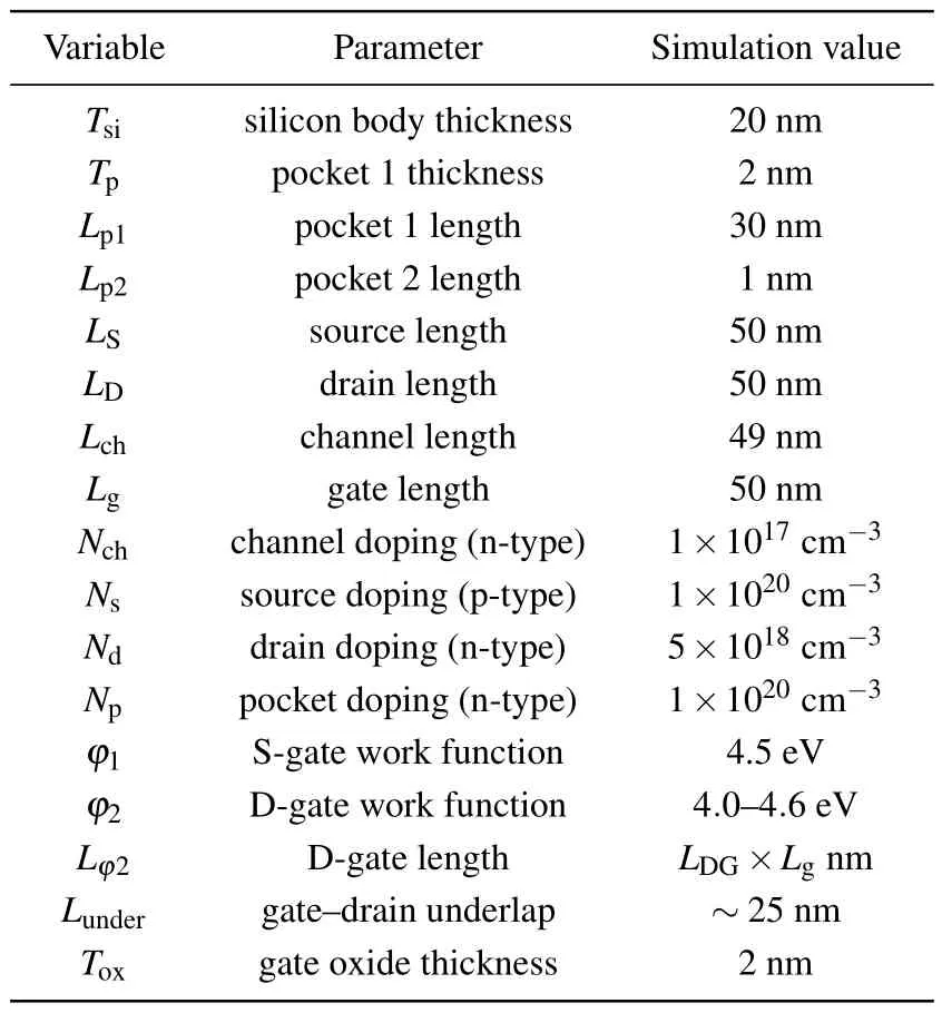
Table 1.The device parameters.
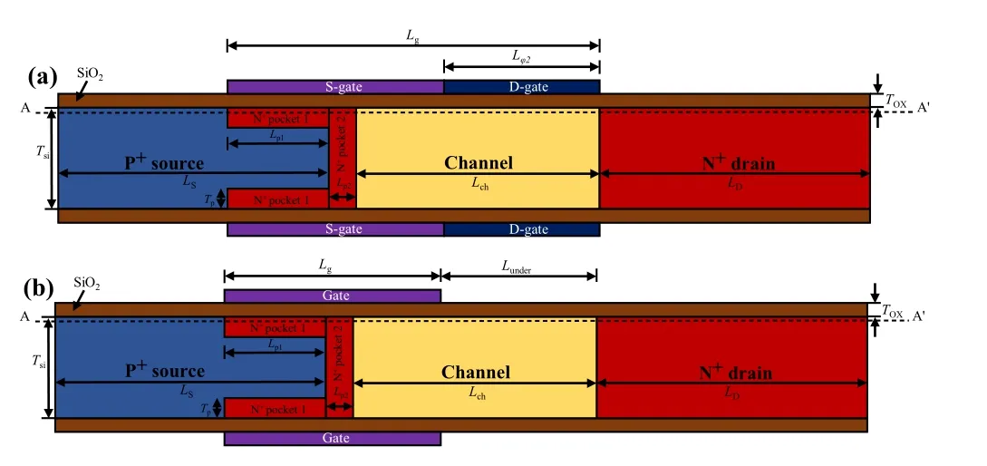
Fig.1.A 2-D schematic view of(a)the CSP-DM-TFET and(b)the CSPUN-TFET.
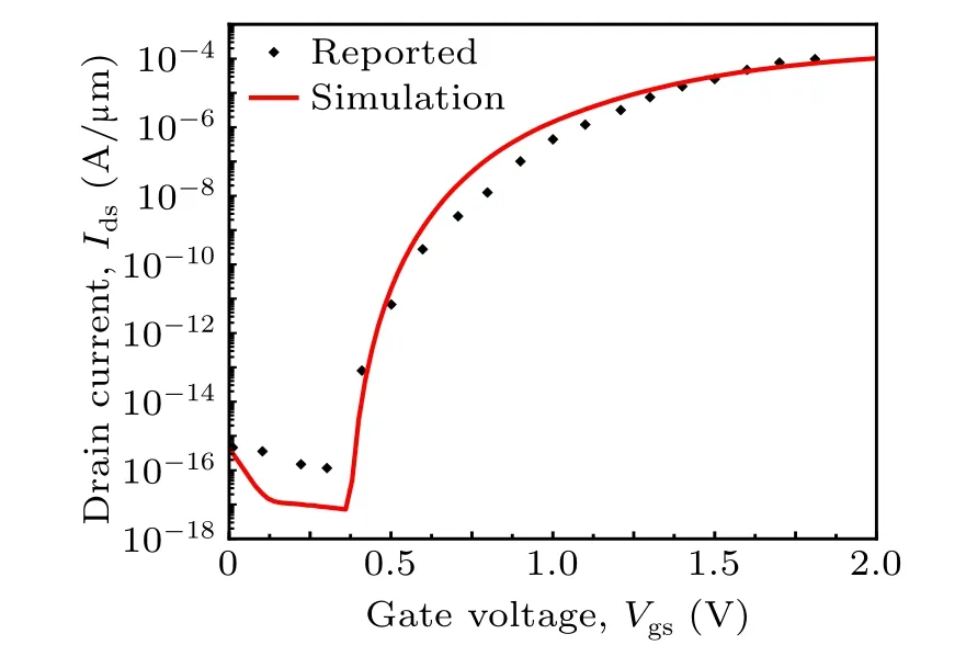
Fig.2.Calibration of the TCAD model parameters obtained by comparing the simulated and experimental Ids-Vgs characteristics of Ref.[3].
3.Results and discussion
The effects of the D-gate work functionφ2, the D-gate lengthLφ2, and the gate-drain underlap lengthLunderon device performance are investigated to obtain better suppression of ambipolar characteristics.TheIon,Iamb,Ion/Ioff,and SSavgare important indicators of DC characteristics, andgm,fT,and GBP are important indicators of analog/RF characteristics.The drain voltageVDSis set to 1 V,and the gate voltageVgsis varied from-1.5 V to 2 V.The currents in the statesVDS=1 V,Vgs=2 V,VDS=1 V,Vgs=-1.5 V andVDS=1 V,Vgs=0 V are defined as the on-state currentIon,the ambipolar currentIamband the off-state currentIoff, respectively.Note that in this work, the energy band diagrams and electric field diagrams are obtained at the location of 1 nm (line A-A'in Fig.1)below the interface of the silicon and gate oxide layer along the channel direction.
3.1.DC characteristics analysis
3.1.1.Effect ofφ2andLφ2on the device
Figure 3 shows the energy band diagram of the CSPTFET device in the on, off, and ambipolar states.When a positive voltage is applied to the gate, the energy band in the channel bends downwards, resulting in a partial overlap between the source valence band and the channel conduction band,and carriers tunneling from the valence band to the conduction band to form a current.This phenomenon is called band-to-band tunneling (BTBT).Similarly, when a negative voltage is applied to the gate, the energy band of the channel bends upwards,causing the drain valence band and the channel conduction band to partially overlap,generating a tunneling current.Since the device conducts in both gate polarities,this characteristic is called ambipolarity.This current is created when a negative voltage is applied to the gate and is called the ambipolar current.Ambipolarity is undesirable as it causes malfunction of the inverter-based logic circuits.[36]
Thus this work takes two designs to suppress ambipolar currents, namely, the dual metal gate and the gate-drain underlap, and analysis the effects of these two designs on the ambipolar characteristics of the CSP-TEFT.The present work focuses on the suppression of ambipolar currents and therefore focuses on the channel-drain junction.
The transmission characteristics of the CSP-DM-TFET are shown in Fig.4.We setLp1as 30 nm andLDGas 0.5(LDGis the D-gate gate length factor,which is the proportion of Dgate to the total channel area gate length), change the D-gate gate work functionφ2from 4.0 eV to 4.6 eV, and keep the S-gate gate work function at 4.5 eV.It can be seen from Fig.4 that the ambipolar current decreases as the D-gate gate work functionφ2decreases.This is due to the fact that as the D-gate work functionφ2continues to decrease,it leads to a reduction in the degree of energy band bending,an increase in the width of the tunneling barrier, and an increasing depletion width at the drain-channel junction, as shown in Fig.5(a), which reduces the incidence of tunneling and suppresses the ambipolar current.

Fig.3.Energy band diagrams of CSP-TFET devices in the on-state(VDS =1 V,Vgs =2 V), off-state (VDS =1 V,Vgs =0 V) and ambipolar state(VDS=1 V,Vgs=-1.5 V),respectively.
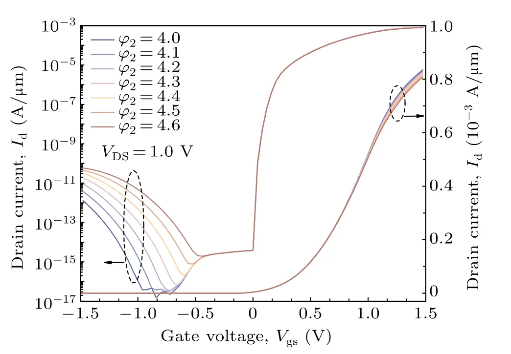
Fig.4.Effects of the work function φ2 on the transmission characteristics of CSP-DM-TFET devices,where the left Y-axis corresponds to the logarithmic curve and the right Y-axis to the linear curve.
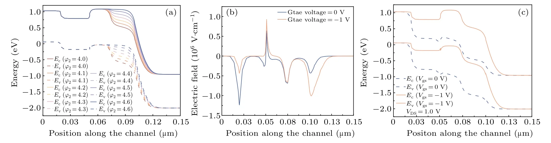
Fig.5.(a) An energy band diagram of the CSP-DM-TFET in the ambipolar state corresponding to the variation of the work function φ2 from 4.0 eV to 4.6 eV (VDS =0 V,Vgs =-1.5 V).(b) The lateral electric field intensity of the CSP-DM-TFET in the off-state (VDS =0 V,Vgs =0 V) and in the ambipolar state(VDS=0 V,Vgs=-1.5 V).(c)An energy band diagram corresponding to the CSP-DM-TFET in the off-state(VDS=0 V,Vgs=0 V)and the ambipolar state(VDS=0 V,Vgs=-1.5 V).
Furthermore,it can be seen from Fig.4 that as the negative gate voltage continues to increase, the ambipolar current shows a decreasing trend and then increases.The reason for this,as shown in Fig.5(b),is that the existence of the C-type pocket, as well as the gate full overlap structure, results in a high lateral electric field in the pocket region of the device in the off-state, leading to a high leakage current.As the negative gate voltage increases, the leakage current is suppressed.In other words, the leakage current is dominant in the negative gate voltage range of 0 V to-1 V.As shown in Fig.5(c),as the negative voltage rises,the energy band gradually bends upwards,the tunneling barrier decreases,and the reverse conduction takes place.At this point,the tunneling current at the drain-channel junction becomes dominant.
To further optimize the CSP-DM-TFET,the effect of theLφ2on the ambipolar and on-state currents is analyzed.TheLφ2is the length of the D-gate and is defined asLDG×Lg(0<LDG≤1).The effect of theLDGon the DC characteristics of the CSP-DM-TFET withLp1at 30 nm,Lp2at 1 nm,andφ1andφ2at 4.5 eV and 4.0 eV, is shown in Fig.6(a).TheLDGvaries from 0.1 to 0.9,with the ambipolar current decreasing with the increasingLDGuntil it goes to 0.6.It can be seen in Fig.6(b) that as theLDGincreases, the degree of energy band bending at the channel/drain junction decreases,leading to an increase in the tunneling barrier and suppression of the ambipolar current.As theLDGcontinues to increase beyond 0.6, there is no significant change in the ambipolar current, but the leakage current in the off-state increases and the device cannot be switched off.As shown in Fig.6(c),due to the increasedLDG, which brings the D-gate with its lower work function closer to the source-channel junction,the electric field strength near the source-channel junction is increased, thus reducing the tunneling barrier width and allowing the device to have a higher leakage current in the off-state.In addition,Ionslightly increases with the increasingLDG.Based on the above analysis, theLDGwas optimally set to 0.6,withIon=9.66×10⁻⁴A/μm,Iamb=6.94×10-17A/μm,SSavg=17.7 mV/dec,andIon/Ioff≈1×1011.In this work,the average subthreshold swing is used as a performance metric.Bhuwalka[37]and Boucart and Ionescu[3]proposed a definition for calculating SSavgwith the following equation:[38]
whereVTHis the threshold voltage,whose value is the voltage corresponding to a drain currentITHof 10-7A/μm.AndVOFFtakes the value of the gate voltage corresponding to a drain currentIoffof 10-14A/μm.
3.1.2.Effect ofLunderon the device
The CSP-UN-TFET retains full overlap of the gate at the source, varying the value of theLunderfrom 5 nm to 25 nm,and its transfer characteristics are shown in Fig.7(a).As the length of theLunderincreases,the ambipolar current decreases.When it reaches 25 nm, the ambipolar current decreases by about six orders of scale.As shown in Fig.7(b),the decreased ambipolar current is caused by gate-drain underlap,which results in a reduced electric field at the channel/drain junction.As theLunderincreases,the electric field density at the channeldrain junction becomes smaller,which reduces the probability of tunneling and thus suppresses the ambipolar current.In addition, from the energy band diagram, as shown in Fig.7(c),the energy band bending at the channel-drain junction decreases as theLunderincreases, which increases the width of the tunneling barrier.Similarly, when theLunderis 25 nm,the ambipolar current decreases with an increasing negative gate voltage in the 0 to-1 V range.Because the leakage current dominates in this range, there is a relatively small increase in the tunneling current at the channel/drain junction.As the negative gate voltage continues to increase after-1 V,the tunneling current at the channel/drain junction dominates,at which point it rises slightly as the negative gate voltage increases.Compared to the CSP-DM-TFET,the CSP-UN-TFET is more effective at suppressing ambipolar currents,which remains low by~10-16orders of scale at the gate voltage of-1.5 V.Furthermore, as shown in Fig.7(a), the on-state currentIondecreases as the length of theLunderincreases, but the reduction is limited.Therefore, to suppress the ambipolar current more effectively, theLunderlength is set to 25 nm.The DC characteristics of the CSP-UN-TFET device in this case areIon=8.34×10⁻⁴A/μm,Iamb=2.79×10-17A/μm,SSavg=16.9 mV/dec,andIon/Ioff≈1×1011.
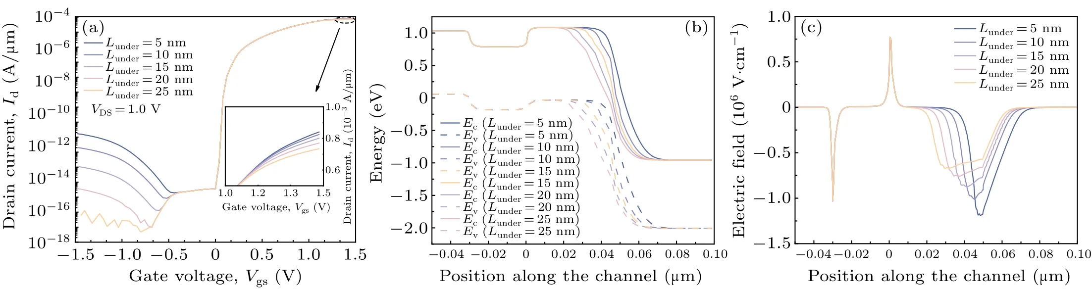
Fig.7.(a)The effect of the Lunder change from 5 nm to 25 nm on the transfer characteristics of CSP-UN-TFET devices.CSP-UN-TFET devices in the ambipolar state(VDS=1 V,Vgs=-1.5 V)with the Lunder change from 5 nm to 25 nm,corresponding to(b)the energy band diagram,and(c)the lateral electric field.
In summary, the ambipolar characteristics of both the CSP-DM-TFET and CSP-UN-TFET devices are suppressed.But compared to the CSP-DM-TFET,the CSP-UN-TFET can suppress the ambipolar current better with the disadvantage of the reducedIon.
Therefore,to ensure that the ambipolar currents are suppressed without affecting the on-state currents as much as possible,a combination of these two methods is used to compensate for the negative effects on the on-state currents caused by the gate-drain underlap structure.During the combination process of optimization,the following principles were applied: minimal reduction of the on-state current and complete suppression of the ambipolar current.The finalized improved device CSP-DMUN-TFET structure is shown in Fig.8.The device parameters are:LDGof 0.4,Lunderof 20 nm, andφ2of 4.0.Figure 9 shows a comparison of the transfer characteristic curves of the CSP-DM-TFET, CSP-UN-TFET, and CSP-DMUN-TFET devices.It can be seen that the ambipolar current of the CSP-DMUN-TFET device remains at the same level as that of the CSP-UN-TFET, and theIonof the CSPDMUN-TFET is larger than that of the CSP-UN-TFET.In this case,the DC characteristics of the CSP-DMUN-TFET device areIon=9.03×10⁻⁴A/μm,Iamb=2.15×10-17A/μm,SSavg=13.3 mV/dec,andIon/Ioff≈1×1011.
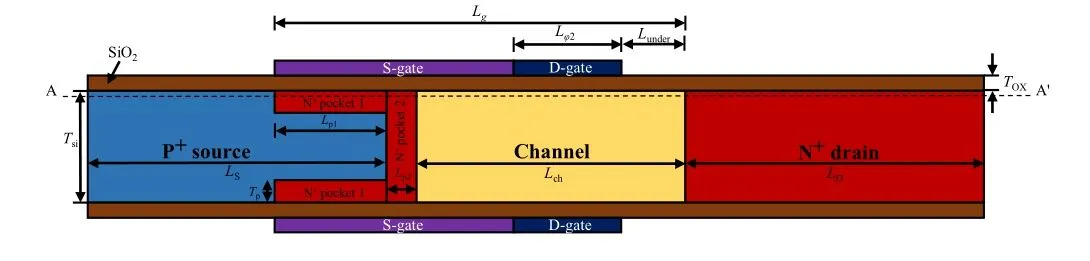
Fig.8.A 2-D schematic view of the CSP-DMUN-TFET.
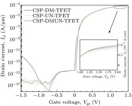
Fig.9.A comparison of transmission characteristics curves for the CSPDM-TFET,CSP-UN-TFET,and CSP-DMUN-TFET devices.
3.2.Analog/RF characteristics analysis
In this section, the effects ofφ2andLunderon the analog/RF characteristics of the CSP-DM-TFET and CSP-UNTFET devices are investigated,including the transconductance(gm), cut-off frequency(fT), gain-bandwidth product(GBP),etc., respectively.These parameters are extracted at the frequency of 1 MHz.Thegmis an important indicator that is used to measure the analog characteristics of devices,[39]and a highergmindicates better performance for analog applications.Analysis of the analog parametergmplays a critical role in obtaining a higherfTand GBP.[40]
Figures 10(a)and 10(b)shows the effect ofφ2andLunderparameters on thegmof the CSP-DM-TFET and CSP-UNTFET devices, respectively.It can be seen from Figs.10(a)and 10(b)that as the gate voltage increases, the drain current increases,which leads to an increase in thegm.However,due to the decrease in carrier mobility, the higher theVgsvoltage is, the lower thegmis.Furthermore, it can be noted that theLunderhas a greater effect on thegmthan theφ2, as a largerLunderreduces the drain current.
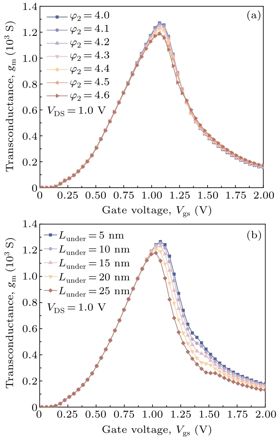
Fig.10.(a)Variation of φ2 from 4.0 eV to 4.6 eV,corresponding to the gm of the CSP-DM-TFET device.(b) Variation of Lunder from 5 nm to 25 nm,corresponding to the gm of the CSP-UN-TFET device.
Figures 11(a)and 11(b)show the effect ofφ2andLunderon theCgdof the CSP-DM-TFET and CSP-UN-TFET devices,respectively.It can be seen from Fig.11(a)that varying theφ2has a greater effect on theCgdof the CSP-DM-TFET device at low voltages.As the lower work function increases, the coupling between the gate and drain,Cgd,gradually increases asφ2decreases, affecting the switching speed of the device.In addition, theCgddecreases with the increasingLunder, as seen in Fig.11(b), due to the fact that the gate-drain underlap structure increases the distance between the gate and drain regions,weakens the capacitive coupling,and reduces the effective charge concentration in the uncovered region of the gate.[41,42]
The cut-off frequency is the frequency at which the current gain becomes unity, and plays a significant role in deciding the device performance at high frequency,[43]as shown below:
As can be seen from Eq.(2),fTis positively proportional togmand inversely proportional toCgg.
As shown in Fig.12,thefTincreases as theVgsincreases initially and after thefTreaches its peak, it begins to fall sharply, due to the fact that thegmbegins to fall after reaching its maximum value and is accompanied by an increase in theCgd.From Fig.12(a), it can be seen that changing theφ2has an apparent effect on thefTof the CSP-DM-TFET device,due to the fact that a decrease in theφ2increases the coupling between the gate-drain and theCgdincreases.When theφ2is 4.0 eV,it obviously reduces the cut-off frequency of the CSPDM-TFET.Figure 12(b) shows that the effect of theLunderis not very significant on thefT, because both thegmin the numerator and theCgdin the denominator decrease as theLunderincreases.
Another important parameter for RF analysis is the GBP,which signifies the product of gain and bandwidth at a constant DC gain value 10.[44]The value of the GBP is expressed as follows:
As shown in Figs.12(c)and 12(d),the tendency of the GBP is similar to that of thefT.
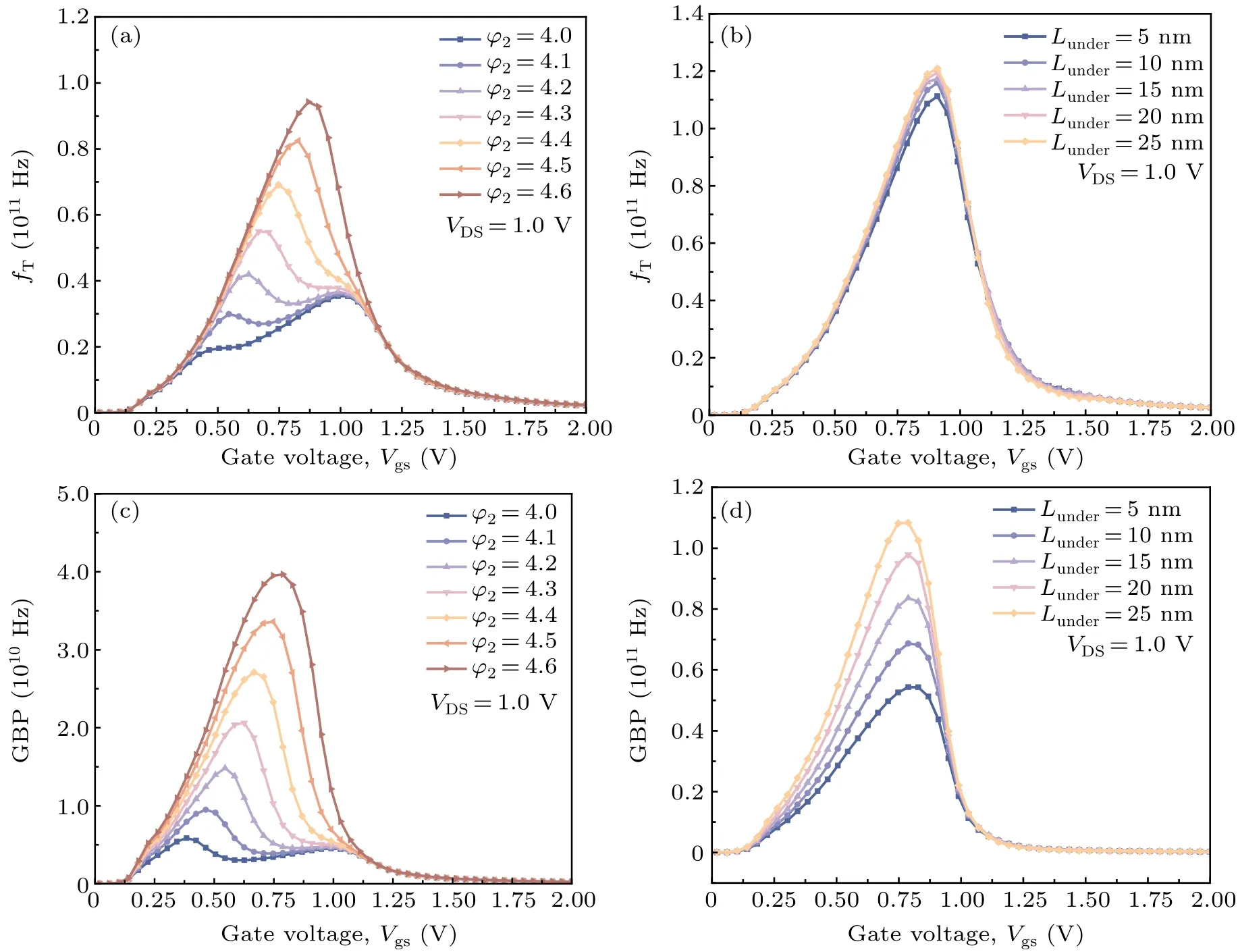
Fig.12.(a)and(c)The change of φ2 from 4.0 eV to 4.6 eV,corresponding to the variation of the fT and GBP of the CSP-DM-TFET device,respectively.(b) and (d) The change of Lunder from 5 nm to 25 nm, corresponding to the variation of the fT and GBP of the CSP-UN-TFET device,respectively.
In summary,the CSP-DM-TFET device reduces the analog/RF characteristics by increasing the gate-drain capacitance due to the use of a lower work function in the D-gate.The CSP-UN-TFET improves the analog/RF performance by reducing the gate drain capacitance due to the presence of the underlap in the gate-drain.The CSP-DMUN-TFET device proposed in this work combines the advantages of both designs,with an analog/RF performance somewhere between the above two devices:gm=1.27×10⁻³S,fT=5.99×10¹⁰Hz,GBP=2.06×10¹⁰Hz.
4.Conclusion and perspectives
This work investigated the effects of dual metal gate and gate-drain underlap designs on the ambipolar characteristics of devices based on silicon-based dual-gate CSP-TFETs.Both designs are capable of suppressing ambipolar currents, with the gate-drain underlap being more effective,but with a small reduction in the on-state current, while the dual metal gate barely effects the on-state current.In addition,the dual metal gate structure causes a degradation of the analog/RF performance of the device compared to the gate-drain underlap structure.Therefore, a combination of both designs is proposed for the CSP-DMUN-TFET.Due to the full gate overlap in the pocket area, the CSP-DMUN-TFET has a high onstate current while being able to fully suppress ambipolar currents:Ion=9.08×10⁻⁴A/μm,Iamb=2.15×10-17A/μm,SSavg=13.3 mV/dec,Ion/Ioff≈1×1011,gm=1.27×10-3S,fT= 5.99×10¹⁰Hz, GBP = 2.06×10¹⁰Hz.The CSPDMUN-TFET effectively solves the problems of low on-state current and ambipolar characteristics of conventional dualgate TFETs and is more suitable for low-power applications.
Acknowledgment
Project supported by the National Natural Science Foundation of China(Grant Nos.52177185 and 62174055).
猜你喜歡
興趣閱讀·少年詩刊(2024年5期)2024-05-22 02:59:58
Plasma Science and Technology(2023年12期)2023-12-18 03:54:50
小讀者·閱世界(2023年8期)2023-08-29 07:36:35
中國應急管理科學(2022年2期)2022-05-23 05:51:18
電化教育研究(2022年3期)2022-04-14 08:20:32
小學生優(yōu)秀作文(低年級)(2020年9期)2020-10-26 09:10:40
作文周刊·小學三年級版(2019年48期)2019-02-02 04:13:00
陜西檔案(2019年5期)2019-01-09 21:58:02
小學生作文·小學中高年級適用(2018年4期)2018-08-15 23:51:04
下一代英才(2018年3期)2018-06-23 11:23:20

- Chinese Physics B的其它文章
- Corrigendum to“Reactive oxygen species in plasma against E.coli cells survival rate”
- Dynamic decision and its complex dynamics analysis of low-carbon supply chain considering risk-aversion under carbon tax policy
- Fully relativistic many-body perturbation energies,transition properties,and lifetimes of lithium-like iron Fe XXIV
- Measurement of the relative neutron sensitivity curve of a LaBr3(Ce)scintillator based on the CSNS Back-n white neutron source
- Kinesin-microtubule interaction reveals the mechanism of kinesin-1 for discriminating the binding site on microtubule
- Multilevel optoelectronic hybrid memory based on N-doped Ge2Sb2Te5 film with low resistance drift and ultrafast speed