
Lower bound on the spread of valley splitting in Si/SiGe quantum wells induced by atomic rearrangement at the interface
2023-11-02 08:12:08GangWang王剛ShanGuan管閃ZhiGangSong宋志剛andJunWeiLuo駱軍委
Chinese Physics B 2023年10期
Gang Wang(王剛), Shan Guan(管閃), Zhi-Gang Song(宋志剛), and Jun-Wei Luo(駱軍委),?
1State Key Laboratory of Superlattices and Microstructures,Institute of Semiconductors,Chinese Academy of Sciences,Beijing 100083,China
2Center of Materials Science and Optoelectronics Engineering,University of Chinese Academy of Sciences,Beijing 100049,China
Keywords: quantum wells,valley splitting,alloy concentration fluctuation
1.Introduction
In the pursuit of universal fault-tolerant quantum computing, the realization of quantum error correction requires a substantial number of qubits that can be effectively controlled and coherently coupled.[1]Leveraging advanced semiconductor fabrication techniques capable of integrating billions of transistors on a single Si chip,[2]electron spins confined in Si quantum dots have emerged as a highly promising platform for quantum computing.[3]Notably, the weak intrinsic spin-orbit interaction and the presence of nuclear zero-spin isotopes contribute to a prolonged coherence time for the electron spin,effectively suppressing both spin relaxation[4,5]and dephasing.[6-8]Despite recent progress[9-16]has been made,Si spin qubits still face the challenge of valley degeneracy,which obstructs the isolation of individual two-level spin-1/2 states[9,10,14,17,18]and introduces a significant leakage channel,thereby impeding high fidelity.[5,19-22]However,the presence of discontinuous heterointerfaces, coupled with strong quantum confinement, can lift the low-lying two-fold valley degeneracy and establish an energy separation known as the valley splitting(EVS).This approach effectively addresses fidelity degradation in spin-only qubits in Si.Unfortunately,the measuredEVSin Si/SiGe quantum wells tends to be relatively narrow,typically around tens to hundreds ofμeV.[23-29]This narrow energy splitting exacerbates challenges related to rapid spin relaxation,[5,19,20]dephasing,[21,22]and errors in spin transport.[30]Moreover,the disorder in the SiGe alloy barrier introduces significant fluctuations in the valley splitting energy, ranging from nearly zero to thousands of μeV.[31-34]Consequently, this poses a significant challenge to the scalability of silicon qubits within the context of universal faulttolerant quantum computing.[34]
Both extensive theoretical work[32,35-49]and experimental observations[24,27,28,34,50-55]have pointed out that theEVSdepends sensitively on the microscopic details near the interface.Particularly, a recent investigation[34]delves into the atomic-scale reconstruction of the Si/SiGe interface and reveals its three-dimensional(3D)morphology,highlighting the microscopic alloying concentration fluctuation along the confinement direction (i.e.,zaxis in Fig.1(a)) as the underlying cause of the substantial spread observed in theEVSmeasurements of various quantum dot devices.However,the in-plane randomness is inevitably ignored in their analysis since the concentration was obtained with its in-plane components averaged in advance,as illustrated in Fig.1(b).It is worth noting that by carefully controlling the epitaxial growth of Si/SiGe heterostructures, the one-dimensional concentration fluctuationδρGe(z) can be effectively minimized to a satisfactory extent, whereas the atomic random distribution within each SiGe barrier layerρGe(x,y) remains uncontrollable.Therefore, the effect of in-plane randomness onEVSis supposed to be more important than the out-of-plane one in terms of device preparation process.Nevertheless, the impact of this type of randomness has been largely disregarded in prior investigations,[35,37-40,43,56-60]partially due to the limitations of the adopted conventional theoretical methods.

Fig.1.(a) The three-dimensional (3D) representation showcasing the landscape of a Si/Si0.7Ge0.3 QW.(b)Schematic diagram illustrating the process of performing in-plane averaging on the concentration fluctuations of Si and Ge atoms within the 3D landscape of Si/Si0.7Ge0.3 to derive the one-dimensional(1D)concentration profiles,ρGe(z).
In this study, we employ the atomistic empirical pseudopotential computation method(EPM)to investigate the impact of alloy disorder on theEVSin Si/SiGe quantum well(QW).Surprisingly,we discover a remarkable and significant spread in theEVS, even in the absence of alloy concentration fluctuation along the quantum confinement direction in Si/SiGe QW.Notably,we find that the minimum extent of the spread inEVSis attributed to the stochastic distribution of Si and Ge atoms within the plane, independent of vertical alloy concentration fluctuations.Moreover, we elucidate the concept of in-plane random distribution of Si and Ge atoms as a consequence of changes in the interface step morphology,providing insights into the occurrence of fluctuation in theEVSinduced by in-plane randomness.Our results thus offer valuable guidance for enhancing the performance of Si-based spin qubits through interface engineering, highlighting the significance of addressing in-plane randomness for achieving improved qubit performance.
2.Atomistic computation method
We calculate the electronic structures of Si/SiGe QWs by directly diagonalizing the band Hamiltonian,which is described by its potential,V(r).This potential encompasses spin-orbit-coupled and nonlocal empirical pseudopotentials.For the system’s pseudopotential, we employ a superposition of screened pseudopotentialsvα(r) of the constituent atom,[61,62]

To emulate the epitaxy growth of a Si/SiGe QW on a Si0.7Ge0.3buffer layer, where the Si QW is subject to biaxial tensile strain,we initially set the in-plane lattice constant of the supercell to the lattice constant of bulk Si0.7Ge0.3,obtained by Vegard’s law.Subsequently, we determine the optimized lattice constant in the vertical direction and atomic equilibrium positions by minimizing the strain energy of the entire supercell through the use of the atomistic valence force field(VFF)method.[71,72]
3.Results and discussions
3.1.Considerable EVS fluctuation in the absence of alloy concentration fluctuation
We first study the impact of alloy concentration fluctuation in the Si0.7Ge0.3barrier on theEVSof Si/Si0.7Ge0.3QWs using EPM.To simulate the actual setups, numerous Si/Si0.7Ge0.3QW structures are constructed through the direct sampling methods and the Si0.7Ge0.3random alloy part comprises 3600 atoms.Each constructed Si/Si0.7Ge0.3QWs feature distinct random alloy configurations within the Si0.7Ge0.3barriers.Consequently,these Si/Si0.7Ge0.3QW structures exhibit varying degrees of alloy concentration fluctuation.To quantify the extent of alloy concentration fluctuation in different Si/Si0.7Ge0.3QW structures, we utilizeσ(ρGe(z))as a measure, as defined in the caption of Fig.2.As illustrated in Figs.2(a)-2(b),the representative Ge concentration profiles clearly show the reduction in size of the alloy concentration fluctuation within the Si/Si0.7Ge0.3QW.Notably, it is challenging to precisely control the magnitude of alloy concentration fluctuation to achieve sufficiently small values through random sampling of the Si0.7Ge0.3barrier.To address this issue,we build Si0.7Ge0.3by spatially restricting the degrees of freedom of the random configuration space.Specifically, we systematically produce a set of Si/Si0.7Ge0.3QWs by maintaining a constant Si-to-Ge atom ratio per atomic monolayer(ML)along the vertical direction.Meanwhile,the distribution of Si and Ge atoms is randomized within each barrier layer.In this way,we obtain the concentration profile of ideal laterally infinite Si/Si0.7Ge0.3QW(see Fig.2(c)).

Upon obtaining a range of Si/Si0.7Ge0.3QW structures with varying degrees of alloy concentration fluctuation, we then carry out calculation to determine the correspondingEVS.Within the atomistic simulation,a 10 MV/m of electric field is applied in the QW confinement direction.There are two reasons for applying an electric field: First, in real SiGe quantum devices, there is typically a perpendicular electric field across the SiGe heterostructure in the order of a few MV/m.Second, it is well studied that the valley splitting in Si/SiGe quantum wells fast decays with an increasing thickness of the quantum well and exhibits oscillations at the atomic scale(~3 ML).[37,38,40,58]To ensure a focused investigation on the electronic states near the interface of one side of the quantum well and avoid the influence of the interface on the other side,an electric field is applied in thez-direction which confines the electronic states to the desired region of interest.However,the presence of an electric field can exacerbate the effect of potential variation resulting from SiGe disorder on the electronic states within the Si quantum well.Specifically,a higher electric field strength can lead to more pronounced fluctuations in the valley splitting in Si/SiGe quantum wells.From Fig.2(d),one observes that an increased degree of alloy concentration fluctuation within the Si/Si0.7Ge0.3QW leads to a greater energy fluctuation ofEVS,as denoted by the green empty circles in Fig.2(d).Moreover, increasing the degree of alloy concentration fluctuation generally increases theEVS.These findings align with the conclusions drawn in Ref.[34],indicating that alloy concentration fluctuation alongzis responsible for the spreading of the energy fluctuation inEVS.However, our atomistic calculations(depicted by the orange empty circles in Fig.2(d))show that,even in the absence of alloy concentration fluctuation within the Si/Si0.7Ge0.3QW, a substantial energy fluctuation inEVS, amounting to±0.33 meV, persists.This significant fluctuation arises solely from the random in-plane distribution of Si and Ge atoms within the Si0.7Ge0.3barrier layer.Remarkably, this fluctuation inEVSis comparable in magnitude to the one caused by the alloy concentration fluctuation.It is crucial to emphasize that while the concentration fluctuation of the Si0.7Ge0.3barrier in the vertical direction can be mitigated through the epitaxial growth of Si/Si0.7Ge0.3heterostructures with low-temperature budget,the atomic random distribution within the SiGe barrier layer remains uncontrollable.Consequently, such a uncertainEVSresulting from the in-plane atomic randomness is an inherent characteristic and represents the lower bound of the energy fluctuation in Si/Si0.7Ge0.3QWs.
It should be clarified that, in the process of generating SiGe random alloys, we deliberately opted for a finite supercell size,a choice that unavoidably introduces some hypothetical order within the SiGe alloys.Nevertheless, we wish to reiterate our stance that our study is primarily centered on the comparative evaluation of the energy ranges associated withEVSvariations within the two distinct Si/SiGe QW structural categories(σ(ρGe(z))/=0 andσ(ρGe(z))=0).The utilization of a finite supercell size inherently contributes to an augmentation of theEVSfluctuation in both classes of Si/SiGe QW structures.However, it is noteworthy that the inherent characteristics of the supercell size exert minimal influence on the relative magnitudes of these energy ranges.Our focus remains directed toward discerning the relative size ofEVSfluctuation between the two aforementioned structural categories.
3.2.Effect of interface atomic step on EVS
Having identified the lower bound of theEVSspread in Si/Si0.7Ge0.3QWs, we next clarify its origin by using a simplified atomic step model.SinceEVSis recognized as an interface-related phenomenon, the in-plane atomic randomness effect within the barrier alloying layer predominantly relies on the behavior of interface roughness.This behavior can be basically described by a sequence of atomic step edges at the interfaces,as depicted in Figs.3(a)-3(b).To streamline the discussion and focus on the impact of a single interface atomic step edge onEVS,we deliberately select pure Ge as the barrier material for the Si QWs,instead of Si0.7Ge0.3.By doing so,we isolate the influence of alloy disorder and direct our attention specifically toward the interface step effect.
We consider a scenario where a one-monolayer-tall(a/4)interface atomic step edge,along they-direction,is positioned atx=γLx(whereais the Si lattice constant andLxrepresents the supercell size in thex-direction), as depicted in Fig.3(c).The calculatedEVSdependent on the step position is plotted in Fig.3(d).Notably, one observes a significant alteration in theEVSwhen the interface step is moved along thexdirection, with the magnitude ofEVSreaching its minimum when the interface step is located at 0.4Lx.
To elucidate the suppressive effect of the interface step onEVS, we establish an effective mass model.The interface atomic step depicted in Fig.3(c)can be conceptualized as dividing one interface (atzI/F) into two halves and vertically shifting one half upward by one ML(a/4).This process gives rise to two laterally distributed half-interfaces,labeled as I/F-1 and I/F-2.When an external electric fieldFis applied along the QW growth(z)direction,the electronic states primarily localize at the upper interface containing the atomic step.The corresponding confinement potential can be expressed as[47,48]
hereεdenotes the dielectric constant and rect(x) represents the rectangle function.[73]The vertical coordinates of the two laterally distributed single interfaces are related byzI/F-2=zI/F-1+.For a single interface(I/F)located atzI/F,the valley coupling matrix can be expressed using the effective mass approximation theory[40,48,60]as follows:
where eiωrepresents an extra phase change induced by the valley coupling.[38]To validate the effective model developed above,we perform a fitting procedure using our atomistic calculation results ofEVSand Eq.(5),with adjustments made to the parametersC,ω, andα/β.The results, as depicted in Fig.3(d),demonstrate the capability of the model,incorporating two laterally distributed interfaces, to accurately describe the impact of the interface atomic step onEVS.The effective model reveals that the atomic-step-position-dependent behavior ofEVSarises from a phase difference e-ik0a/2between the two laterally distributed interfaces, which are vertically separated by one ML.
3.3.Effect of in-plane random distribution of Si,Ge atoms on EVS
The effective model can be easily extended to investigate scenarios involving multiple interface atomic steps,which contain the changes in the surface topography and can largely reflect the in-plane random distribution of Si and Ge atoms in the absence of alloy concentration fluctuations along the quantum confinement axis.To explore the effects of multiple interface atomic steps onEVS, we initially consider the case of a single interface step positioned atγLx, where the Ge concentration in the nearest neighboring SiGe atomic layer to the Si QW isγ.In order to approximate the random distribution of Si and Ge atoms within the SiGe layer while maintaining a constant Ge concentration, we divide the entire width of the in-plane Ge section,observed in the case of a single step,into two sections separated by a distance ofλLx, as depicted in Fig.4(a).This separation generates four interface segments,each characterized by its vertical coordinatezI/F-i,center positionxiand widthwialong thexdirection.As a result, the QW potential takes on a specific form denoted as

Having determined the parametersC,ω, andα/βin Eq.(5)through fitting the results of atomistic simulations, we can readily compute theEVSfor multiple interface steps using the derived equation
Figure 4(b)represents the dependence ofEVSon two factors:the fractional width of the in-plane Ge section before the step separation,denoted asγ,and the fractional distance of the step separation,denoted asλ.It is evident that,for a fixedγcorresponding to the intra-layer Ge concentration,varying the separation distancesλleads to distinct values ofEVS.This observation underscores how the rearrangement of Si and Ge atoms within a 1 ML-thick interface layer can induce changes inEVS.

Fig.4.(a)A schematic diagram illustrating the separation of interface atomic steps.The initial in-plane Ge section with a width of γLx is equally divided into two subsections,which are separated by a distance of λLx.(b)The valley splitting energy is calculated using the step separation model,represented by Eq.(8).The parameters C,ω,and α/β in Eq.(8)(multiple steps)are consistent with those in Eq.(5)(single step).The variation of EVS is shown as a function of the fractional width of the in-plane Ge section before the step separation, denoted as γ, and the fractional separation spacing,denoted as λ.The values of γ and λ adhere to the constraint γ+λ <1.
3.4.Eliminating the EVS fluctuation caused by in-plane random distribution of Si,Ge atoms
Based on the preceding discussions,it is evident that the fluctuation of valley splitting induced by in-plane randomness imposes a lower limit on the wide spectrum ofEVSin Si/Si0.7Ge0.3QWs,presenting a challenge to the integration of Si electron spin qubits.To tackle this issue,we explore strategies to mitigate this lower limit through interface engineering.Our proposed approach involves the epitaxial growth of a thin Ge layer before the heterogeneous growth of Si0.7Ge0.3on the Si active layer.The inclusion of a thin Ge layer at the Si/Si0.7Ge0.3interface effectively separates the Si well and SiGe barrier, ensuring that the wave function ofΔ±zvalley states remains immune to in-plane potential fluctuations arising from the disorder in the distribution of Si and Ge atoms within the Si0.7Ge0.3barrier layer, as depicted in Figs.5(a)-5(b).Consequently,both the valley coupling and valley splitting in the Si active layer remain unaffected by the disorder within the Si0.7Ge0.3barrier.We substantiate this proposition through atomistic EPM simulations,as illustrated in Fig.5(c).These simulations demonstrate an exponential reduction in the fluctuation ofEVSresulting from the random distribution of Si and Ge atoms within the Si0.7Ge0.3barrier layer as the thickness of the interfacial Ge layer increases.Remarkably, the introduction of a 4-ML thick interfacial Ge layer diminishes the fluctuation inEVSto one-tenth of its original magnitude.It is worth emphasizing that our prior calculations[33,74]have shown a significant amplification ofEVSwith the incorporation of a 4-ML thick Ge layer at the Si QW interface,and this result has also been experimentally validated.[75]

Fig.5.(a) Schematic diagram illustrating the structure of the Si/Si0.7Ge0.3 QW is presented,where the white solid line represents the distribution of Ge concentration, while the red and blue solid lines depict the wave functions of the split Δ±z valley states.(b) Schematic diagram showcasing the structure of the Si/nGe-thick Ge/Si0.7Ge0.3 QW is displayed,with emphasis on the Ge concentration profile and the wave function of the split Δ±z valley states.(c)The energy fluctuation of valley splitting,resulting from the in-plane random distribution of Si and Ge atoms near the Si/Si0.7Ge0.3 interface in the Si0.7Ge0.3 barrier, is effectively mitigated through the insertion of a few Ge layers at the interface.The magnitude of EVS fluctuation,quantified by δEVS,is plotted on the vertical axis,while the thickness of the inserted Ge layer in monolayers(ML)is shown on the horizontal axis. δEVSLB at nGe=0ML is the lower bound of EVS fluctuation in Si/Si0.7Ge0.3 QWs,labeled with superscript“LB”.
4.Conclusions
Our investigation has provided significant insights into the phenomenon ofEVSin Si/SiGe QWs.Surprisingly, we have demonstrated that a substantial spread ofEVScan occur even in the absence of concentration fluctuation.This spread, which arises solely from the in-plane random distribution of Si and Ge atoms within the SiGe barrier,represents the lower bound of the wide spectrum ofEVSobserved in various Si/SiGe devices.We have developed effective atomic step models to describe the impact of in-plane disorder onEVS.By recognizing and incorporating the influence of in-plane randomness, we propose an experimentally feasible method to mitigate the fluctuation ofEVSthrough the design of the interface atomic structure.Specifically, we suggest the inclusion of a thin Ge layer at the Si/SiGe interface, which effectively reduces the alloying-disorder-inducedEVSfluctuations.Our study thus paves the way for the development of more reliable Si-based electron spin qubits.
Appendix A:Local interface induced valley coupling

where the periodic Bloch waves are expanded as plane wavesu±(r)=, andΣdenotes the summation of coefficients of plane wavesΣ=,here onlyG1=G2case is considered sinceG1/=G2terms would lead to fast oscillations in the integrand that average to zero.In Eq.(A1)we integrate by parts the first term
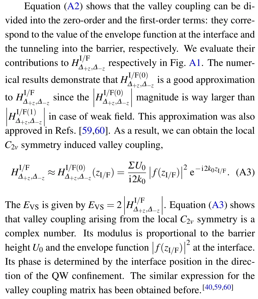

Fig.A1.The contribution of each term in Eq.(A2).The thickness of Si/Ge QW is 10 nm.The barrier height is 150 meV.For the summation of the plane expansion coefficients of Bloch waves,Σ=-0.2607.[48,60]
Acknowledgements
Project supported by the National Science Fund for Distinguished Young Scholars (Grant No.11925407), the Basic Science Center Program of the National Natural Science Foundation of China(Grant No.61888102),and the Key Research Program of Frontier Sciences of CAS(Grant No.ZDBS-LYJSC019), and CAS Project for Young Scientists in Basic Research(Grant No.YSBR-026).
猜你喜歡
公民與法治(2020年13期)2020-07-27 01:30:32
軍營文化天地(2016年3期)2016-05-25 09:38:17
小小說大世界(2015年9期)2015-09-09 03:01:08
軍事歷史(2015年2期)2015-05-21 06:35:38
小朋友·聰明學堂(2014年2期)2014-07-23 09:58:45
意林(2010年11期)2010-05-14 16:48:46
文藝生活·智慧幽默(2007年6期)2007-06-27 09:39:42
故事林(2007年2期)2007-05-14 15:37:47
軍事歷史(2001年6期)2001-08-21 06:50:32
軍事歷史(1993年6期)1993-08-16 02:18:44

- Chinese Physics B的其它文章
- Corrigendum to“Reactive oxygen species in plasma against E.coli cells survival rate”
- Dynamic decision and its complex dynamics analysis of low-carbon supply chain considering risk-aversion under carbon tax policy
- Fully relativistic many-body perturbation energies,transition properties,and lifetimes of lithium-like iron Fe XXIV
- Measurement of the relative neutron sensitivity curve of a LaBr3(Ce)scintillator based on the CSNS Back-n white neutron source
- Kinesin-microtubule interaction reveals the mechanism of kinesin-1 for discriminating the binding site on microtubule
- Multilevel optoelectronic hybrid memory based on N-doped Ge2Sb2Te5 film with low resistance drift and ultrafast speed