
Butt-joint regrowth method by MOCVD for integration of evanescent wave coupled photodetector and multi-quantum well semiconductor optical amplifier
2022-04-12 03:45:02FengXiao肖峰QinHan韓勤HanYe葉焓ShuaiWang王帥ZiQingLu陸子晴andFanXiao肖帆
Chinese Physics B 2022年4期
關(guān)鍵詞:王帥
Feng Xiao(肖峰) Qin Han(韓勤) Han Ye(葉焓)Shuai Wang(王帥) Zi-Qing Lu(陸子晴) and Fan Xiao(肖帆)
1State Key Laboratory of Integrated Optoelectronics,Institute of Semiconductors,Chinese Academy of Sciences,Beijing 100083,China
2College of Materials Science and Opto-Electronic Technology,University of Chinese Academy of Sciences,Beijing 100049,China
Keywords: butt-joint regrowth,etching profile,non-reentrant mesa,photonic integration
1. Introduction
Explosive increase in network traffic in recent years has put forward higher requirements for the existing communication infrastructures. Due to its small footprint, low coupling loss and cost, photonic integrated circuit (PIC) is one of the most important technologies that can satisfy the demand for high communication capacity.[1]PIC on indium phosphide platform[2]has always been the research focus,[3-6]because of its ability of integrating laser and detector on a single chip.For the realization of InP PICs, it is critical to achieve the compatibility of devices with different structures and materials. One way to integrate different materials is to grow materials successively in-plane, which is known as butt-joint regrowth. So far, various kinds of butt-joint integration have been reported,such as InP/InGaAsP waveguide,[7]InGaAsPInGaAlAs integration[8]and InP/AlGaInAs/InGaAsP all active components.[9]Particularly, the realization of SOA/waveguide butt-joints ensures the integration of SOA and evanescent wave coupled photodetector without further growth steps.[10]However, few details of SOA/waveguide butt-joint regrowth have been reported on MOCVD platform.
In this paper, we report a study of butt-joint regrowth of thick passive waveguide layers to SOA mesas, using low pressure metal-organic chemical vapor-phase deposition. To obtain non-reentrant mesas with smooth sidewalls before regrowth,we have conducted two different nonselective etchants on dry etched mesas and found a simple one-step etching method. The morphologies of mesas after wet chemical etching and regrowth are observed by scanning electron microscopy. By comparing the growth morphology and simulating optical transmission along different directions,we have found that waveguides should travel across regrowth interface along the [110] direction. In addition, the dependence of growth rate enhancement on the mask layout has been studied by varying mask dimension and their spacing. The results offer an important guidance for future mask design and vertical alignment between active and passive cores. Based on our method, integrated ECPD and SOA has been fabricated without further regrowth steps, whose high responsivity and low butt-joint interface insertion loss demonstrate a promising future of this technology.
2. Experiment procedure
2.1. Growth of MQW SOA layer structure
The major procedure of our experiment is shown in Fig. 1. The structure of InGaAsP MQW SOA (Fig. 1(a))and InP/InGaAsP regrowth (Fig. 1(d)) were carried out on semi-insulating Fe-doped and(001)-oriented InP substrate by using a low pressure MOCVD reactor. The reactor pressure was 50 mbar. The entire SOA epilayers were first grown at the temperature of 650°C and growth rate of 5 °A/s. Details are presented in Table 1.
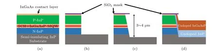
Fig.1. The procedure of regrowth. (a)Growth of MQW SOA layer structure. (b)Dry etching of SOA.(c)Forming a reentrant mesa shape by wet etching. (d)Regrowth of passive waveguide layers around deep etched mesas.
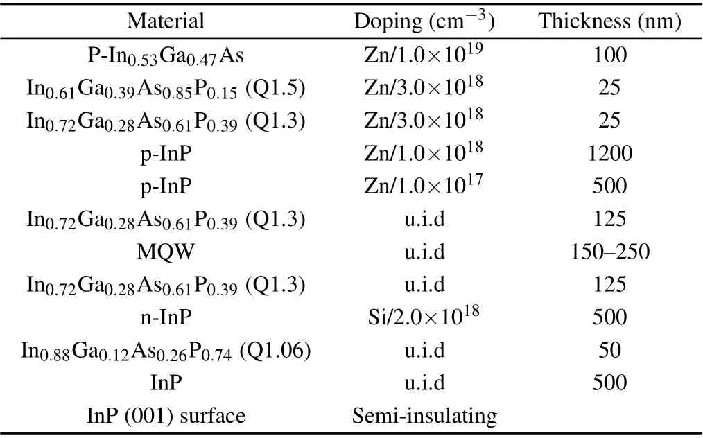
Table 1. Epitaxial structure of MQW SOA.
2.2. Definition of mesa shape
A non-reentrant mesa profile[11]and overhanging SiO2masks[12](as shown in Fig.1(c))before regrowth are helpful to suppress mask overgrowth and achieve surface planarity.The non-reentrant mesa means that the narrowest portion of the mesa is at the top in contact with the mask. The mask overhang over this kind of mesa forms a sharp corner at the top of the mesa, screens the mesa top from the ambient and limits the concentration of reactants available for growth. The growth rate is then significantly reduced at the mesa top so that the top end of the growing layer from the mesa sidewall remains under the mask until the growth on the base plane is planarized,preventing the occurrence of mask overgrowth. To obtain a non-reentrant mesa with mask overhang, pure nonselective wet etching was the most common method.[11-16]However,due to the nature of diffusion-limited reaction during the etching,[17]supply of etchants is more abundant near mask edge. Sunken grooves are usually produced around the mask edges. Regrown waveguide layers on this kind of profiles are not flat enough to obtain practical optical coupling efficiency,and thus preclude the implement of integration of passive waveguides and laser structures. In this study,a two-step etching method, i.e., a combination of III-V inductively coupled plasma etching and wet chemical etching is employed.
As shown in Fig. 1(b), a 500-600 nm thick SiO2was deposited by using plasma enhanced chemical vapor deposition (PECVD) and patterned by means of conventional photolithography. In order to remove the entire SOA epitaxial layers outside masked areas, we have firstly employed Cl2/Ar/CH4III-V inductively coupled plasma etching(Fig. 1(b)) and after that, a wet chemical etching (Fig. 1(c)).Figure 2 shows the etched profiles after ICP etching. The profiles along[110]and[1ˉ10]are almost identical due to the anisotropy of ICP etching. Details of wet etchants we used in this study are listed in Table 2.
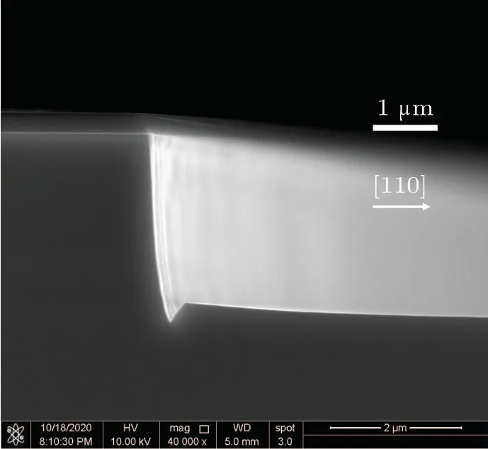
Fig.2. Etched profile of SOA mesas by ICP etching.
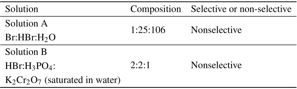
Table 2. Etchants used to define mesa shape.
Solutions A and B are all HBr-based non-selective etchants. All etchings are carried out at the temperature of 0°C without stirring and under ambient illumination.
2.3. Regrowth of passive waveguide layers around deep etched mesas
After etching all the unprotected epi-layer down to the substrate, the wafer was rinsed in oxygen plasma and etched in concentrated H2SO4for 2 min to remove any organic contamination, surface damage and native oxide layer. Finally, one undoped InP layer and one undoped waveguide core layer In0.88Ga0.12As0.26P0.74were regrown.The In0.88Ga0.12As0.26P0.74layer was lattice-matched material with a bandgap of 1.06μm.
3. Result and discussion
3.1. Choice of non-selective etchants
In this study,the ICP etching went through the entire laser epi-layers and stopped in the semi-insulating substrate. The mesa after ICP etching is 2.7-2.8 μm high. Then the wafer went through a one-step non-selective etching.Figure 3 shows the etched profiles of non-selective etchants A and B.
Results of non-selective etching As can be seen from Fig.3,etched profiles on mesas differ dramatically from those on (001) flat surfaces without mesa. The etch rate at the top of mesa is quite higher than that at the bottom of the mesa.For example,in Fig.3(c),the lateral etch depth,i.e.,the mask overhang at the top of mesa is 900 nm,while the etch depth at the bottom of mesa is 300 nm.This phenomenon has also been studied by Fanget al.[18]All mesas along both directions exhibit non-reentrant profiles. In addition,the surface near mesa sidewall is groove-free and connects to the sidewall through a very small inclined angle.
The etching profiles along the[1ˉ10]and[110]directions are different. Along the [110] direction, the sidewall profile exhibits crystal behaviors.However,as for the[1ˉ10]direction,round corners are main characteristics.
Etchant B is more suitable than etchant A to obtain a smooth sidewall profile. When etch time is short(30 s),there is a bump of p-InP on the sidewall along [110] for the case of etchant A(Fig.3(a)). The bump is even shaper and bigger along the[1ˉ10]direction(Fig.3(e)). The bump may affect the material quality of regrowth[19]and even cause optical absorption.Interestingly,it is found that the bump seems to disappear after longer etch time, as can be seen in Figs. 3(b) and 3(f).This phenomenon has not been reported by other researchers before. However, when using etchant B, the sidewall profile is quite smooth along both crystal directions, even at a short etching time(see Figs.3(e)and 3(g)).
Discussion The non-selective scheme after dry-etching is extremely helpful in obtaining non-reentrant mesa configuration. This non-reentrant profile differs from that by pure non-selective etching. The nearly flat surface near sidewall makes it highly feasible to regrow flat waveguide layers and develop novel butt-joint integration process. The bump occurred on sidewall may be caused by unequal etching rate of different materials on the sidewall surface. As a result, the choice of etchant is essential in one-step non-selective etching. The shrinking of InP bump after long etching time may be explained by diffusion and supply of reactants.The bump is closer to the mask edge when mask overhang becomes large.It takes shorter time for reactants to diffuse to the top of mesa than to bump portion. On the other hand, due to the blocking effect of mask, supply of etchants to the top of mesa is much reduced. Consequently, the concentration of reactants near the top of mesa is much lower than that near bump area.Etching rate near top of mesa drops down and the bump disappears gradually. Although a long etching time can help to smoothen the sidewall, the drawback is that thicker InP will be regrown under waveguide core layer to assure alignment with the MQW region. Thicker InP means longer regrowth time, which will accelerate the inter-diffusion and intermixing of dopants, especially in MQW layer. Those effects may deteriorate the performance of device. In short, the morphology produced by etchant B is smoother and its mesa height is lower. Therefore, etchant B, BPK-221 system is the best etchant we could find to date.
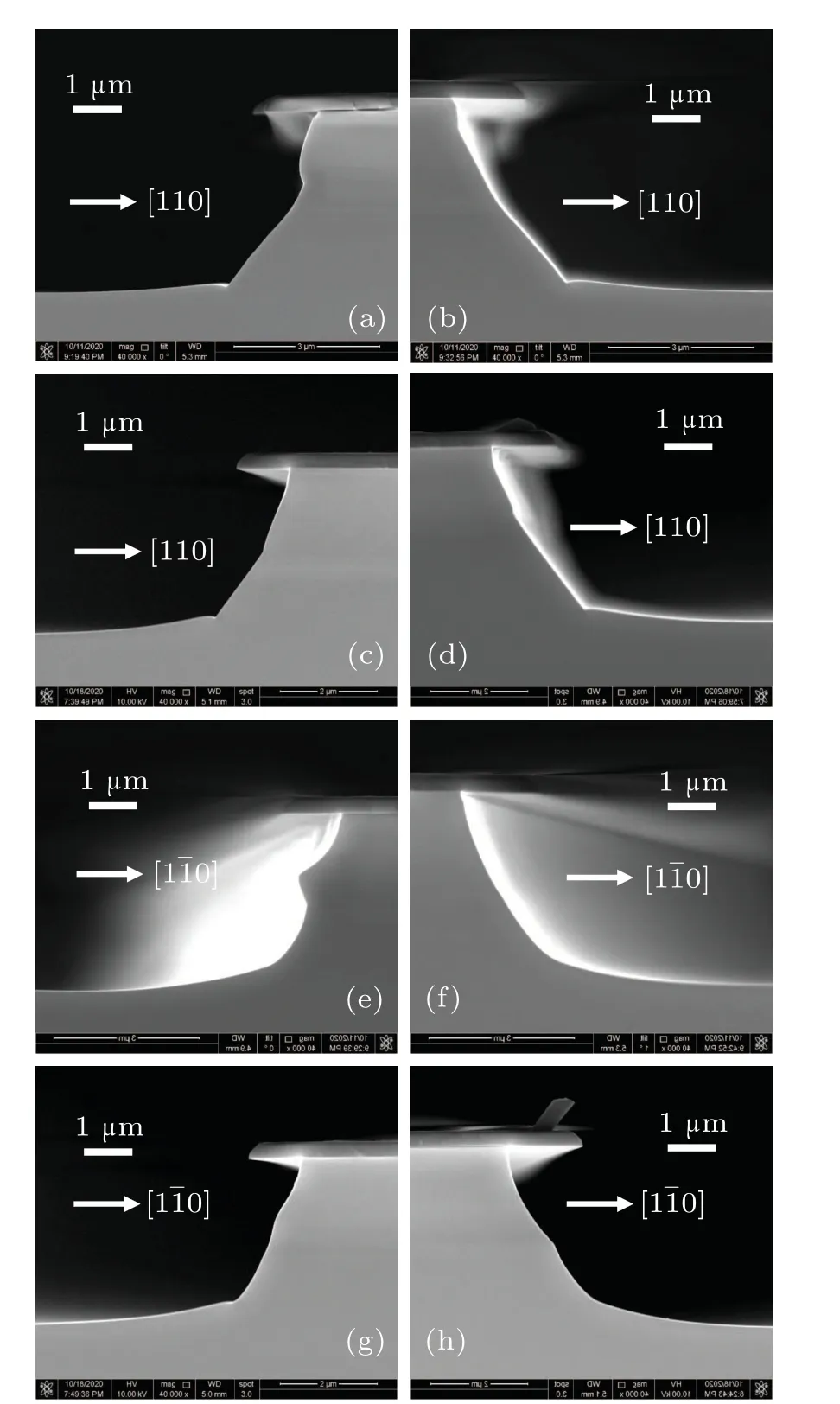
Fig.3. Etched profiles of ICP etched mesa using etchant A and B.(a)30 s in A along [110]; (b) 60 s in A along [110]; (c) 30 s in B along[110];(d)60 s in B along[110];(e)30 s in A along[1ˉ10];(f)60 s in A along[1ˉ10];(g)30 s in B along[1ˉ10];(h)60 s in B along[1ˉ10].
3.2. Regrowth profiles
Figure 4 shows the profiles after regrowth along the[1ˉ10](a)and[110](b)directions. In order to increase the diffusion length of reactants,a high growth temperature of 680°C was used. The reactor pressure was 50 mbar and growth rates for InP and Q1.06 were both 5 °A/s. The growth thickness for InP and Q1.06 were 900 nm and 1000 nm,respectively. The SiO2masks were rectangle stripes.
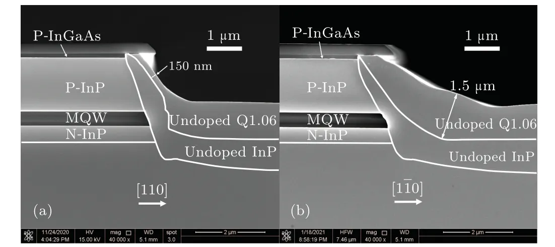
Fig.4. Growth profiles along[110](a)and[1ˉ10](b)directions. The growth temperature is 680 °C. To delineate boundaries between different layers,samples are stained in 3H2SO4:H2O2:10H2O solution for 20 s. The white lines are added according to the etching boundaries.
Results of regrowth Along the[1ˉ10]direction,the thickness of regrown InP decreases slowly on the gently sloping surface towards the active region. This spatial variation of thickness forms a horizontal and flat surface for Q1.06 layer to be regrown. At the mesa sidewall,the growth thickness of InP and Q1.06 is much reduced with respect to that on the (001)surface. Especially for the Q1.06 layer, the ratio of growth rate on the sidewall to growth rate on (001) surface is about 0.15μm/1μm=0.15. The thickness of InP near MQW region is about 600 nm. This thin layer ensures a negligible expansion of optical field between active and passive waveguide core,thus,a low coupling loss at the butt-joint interface.
Unlike the[110]direction, growth rate on slope surface,i.e.,high index surface,seems to be enhanced along the[1ˉ10]direction. After the growth of InP,the slope of mesa sidewall becomes longer and gentler. As for the Q1.06 near mask edge,its surface is corrugated. Also the thickness on the sidewall can reach 1.5 μm, which is much enhanced than that (1 μm)far away from mask.
Discussion The different growth morphologies along the [110] and [1ˉ10] directions are the result of the different bonding configurations existing on the planes exposed for growth.[20]It is believed that high temperature enhances both surface migration and desorption.[21]The pronounced slower growth rate at sidewall along the[110]direction is likely due to the enhanced P evaporation from the surface. In order to figure out whether the [110] or [1ˉ10] direction is suitable for optical transmission,electrical field distribution and butt-joint efficiency based on real growth morphologies are calculated by using 2D-FDTD method. During the calculation,refractive indices are defined at 1550 nm. A light source of fundamental mode of TE polarization is illuminated at the SOA. The butt-joint efficiency is defined as the ratio of the power collected by passive waveguide fundamental mode to the power of light source. Material in the multi-quantum well region was replaced with Q1.3 to prevent light absorption. Figure 5 shows the calculation results. As can be seen from the figure,when light is transmitted along the direction[110],the distribution of optical field is relatively concentrated in the waveguide core. However,when transmitting along the direction[1-10],the optical field expands greatly after passing through regrowth interface,which is caused by the uneven thickness distribution of Q1.06 core layer. In addition,butt-joint efficiency along the [110] direction (0.87) is higher than that along the[1-10] direction (0.72). Therefore, in subsequent integrated devices, waveguides should be fabricated along the [110] direction.
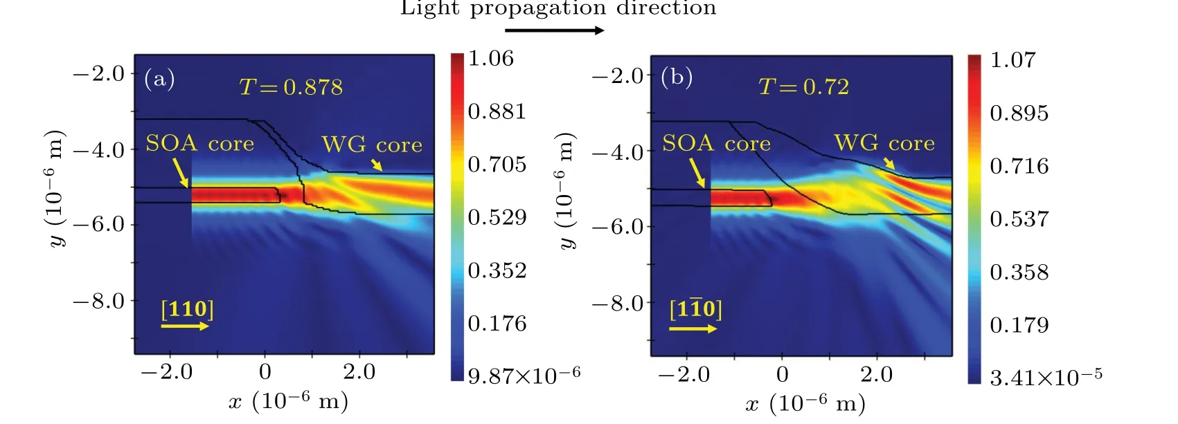
Fig.5. Simulated electrical field profile and butt-joint efficiency based on real growth morphologies along(a)[110]and(b)[1ˉ10]directions.The wavelength and polarization of the light source are 1550 nm and TE respectively. ‘T’in the picture means the butt-joint efficiency.
3.3. The influence of mask layout on growth rate
Since the thickness of regrown layers near mask edge affects the vertical alignment of waveguides, i.e., the coupling efficiency dramatically, it is essential to know how and how much the thickness is affected by the mask design. To examine the influence of mask layout on growth rate along the[110]direction,four samples with different mask designs were grown in the same run with a growth rate of 5 °A/s and a growth temperature of 680°C.Before regrowth,all the samples were etched in BPK-221 solution for 50 s and had mask overhang of 0.8-1.0μm. The mask of active region is rectangular shape and the details are listed in Fig.6 and Table 3. All parameters but one in each sample are kept constant. The long edge was aligned with the [110] direction, along which the waveguide will travel across the regrowth interface. After regrowth,each sample was cleaved along the[110]direction as show in Fig.6.Then thickness of regrown InP and Q1.06 layer was measured at the point 3μm away from mask edge(Fig.7(a))by using the scanning electron microscope.Regrown thicknesses measured on an unmasked substrate are shown in Fig. 7(b). The measured growth thicknesses on the four samples are presented in Fig.7.
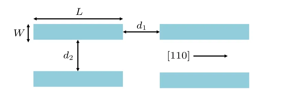
Fig.6. Four design parameters of mask for regrowth. Four parameters are W(width),L(length),d1 (longitudinal spacing)and d2 (transverse spacing).
Table 3. Details of mask design of 4 samples.
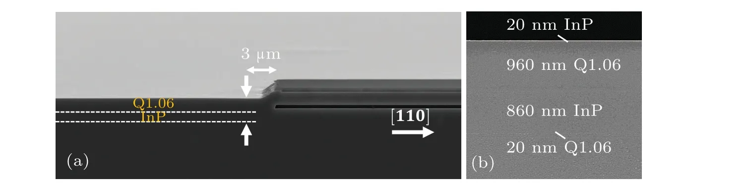
Fig.7. Position(a)where thickness measurements were performed and regrown thicknesses(b)measured on an unmasked substrate.
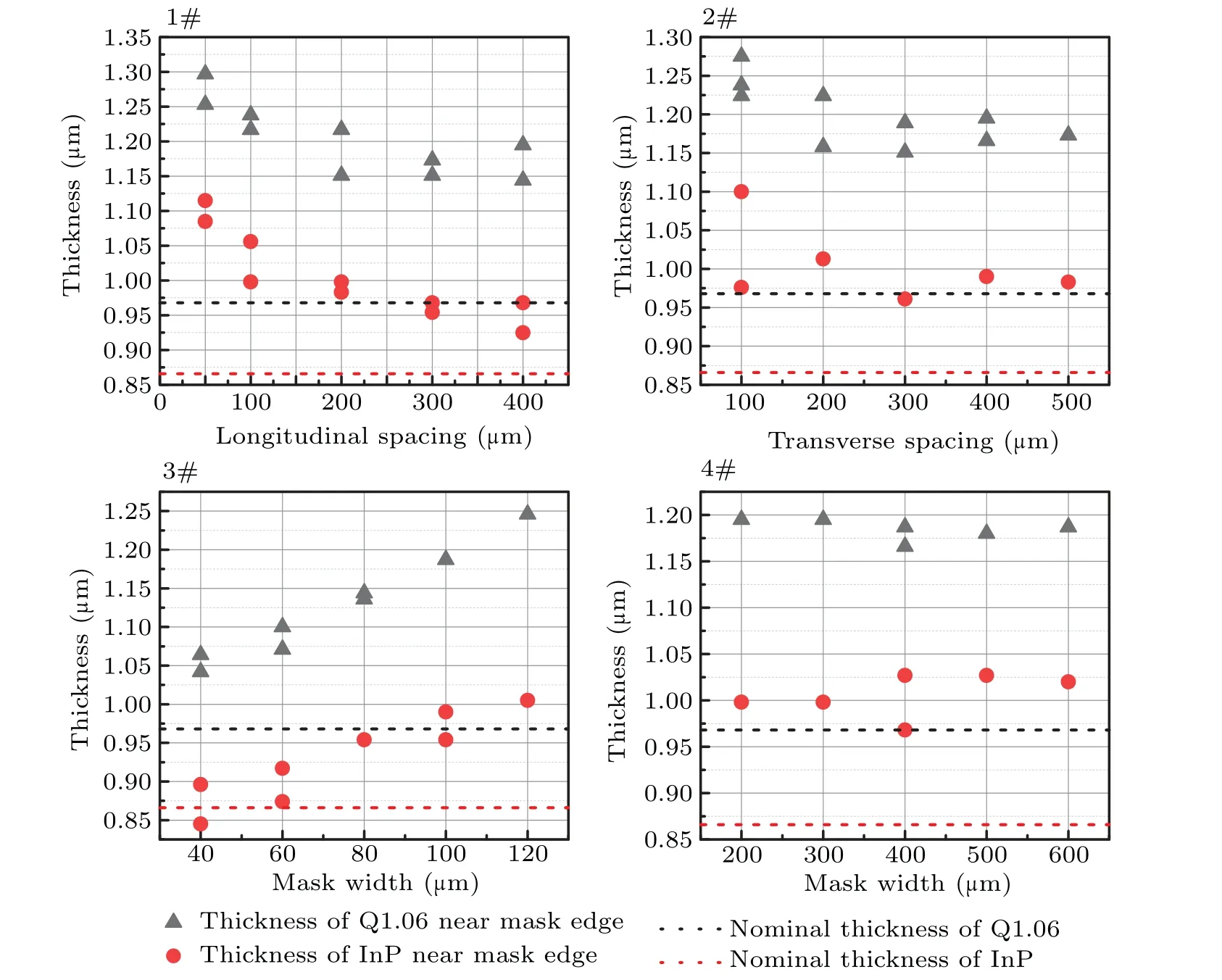
Fig.8. The growth thickness on the four samples.
The growth rate of Q1.06 layer is more enhanced near mask edge than InP material. Here,we define the growth rate enhancement factor[22](GRE)as the ratio of the thickness of the selectively grown layer measured 3 μm away from mask edge and the layer thickness in unperturbated area (nominal thickness in Fig.8). For the case of sample 3,when the mask width is 120 μm, GRE of Q1.06 is 1.25/096=1.30, while GRE of InP is 1.0/0.86=1.16.
The regrowth thickness of Q1.06 and InP layer decreases exponentially with longitudinal and transverse spacing of masks. For the case of sample 1, the thickness of Q1.06 layer dropped from 1.27 μm to 1.18 μm, i.e., a decrease of 90 nm,when longitudinal spacing was increased from 50μm to 200 μm. However, when longitudinal spacing increased from 300 μm to 400 μm, the thickness of Q1.06 was kept around 1.16 μm. Same tendency can be found for InP layer and in sample 2.
The mask width affects the thickness of selectively regrown layers in a linear way,while the mask length seems not to be the deal. For the case of sample 3, the growth thickness of Q1.06 has gained an incremental of 100 nm once mask width was increased by 40μm. As for InP layer,the slope of the relation is 75 nm/40 μm. For the case of sample 4, the growth thickness of Q1.06 has stayed within the rage of 1.18 and 1.20,no matter how long mask length is used. Same tendency can be found for the InP layer.
Discussion The lateral vapor phase diffusion from regions above masks can account for the enhanced growth rate near mask edge for selective area growth. The more enhanced growth rate for Q1.06 than InP may be caused by higher diffusion coefficient of Indium decomposed fragments than gallium decomposed fragments. Thus,more gallium than indium species can be absorbed in region close to masks, increasing the growth rate of Ga-containing material near mask edge.The above results with respect to mask dimensions show that our regrowth process is very useful for monolithic integration of active and passive waveguides. The exponentially decreasing regrown thickness suggests that thickness sensitive devices can work as predicted if they are arranged far enough to the masked active region. The nearly independence of growth thickness on mask length enables a free design of SOA device length without degrading coupling efficiency at regrown interface.
3.4. Device fabrication results
After obtaining controllable butt-joint regrowth on the patterned SOA wafer,regrowth of whole evanescent wave coupled photodetector(ECPD)layer structure around SOA mesa was carried out,by using the same etching method and growth conditions as described in previous sections. In addition to InP/InGaAsP waveguide,the ECPD also includes photodetector(PD)layers,which consist of N-InGaAsP contact layer,i-InGaAs absorbing layer,p-InGaAsP upper cladding layer and P-InGaAs contact layer. Figure 9(a)shows the SEM graph of regrowth profile around butt-joint interface by using a 100μm wide mask. The growth morphology of InP/InGaAsP passive waveguide agrees well with the previous experiment. Although the epitaxial layer of PD has risen above the upper surface of the mask, it does not extend above the mask and exhibits the characteristic of{111}crystal plane at the mask boundary.
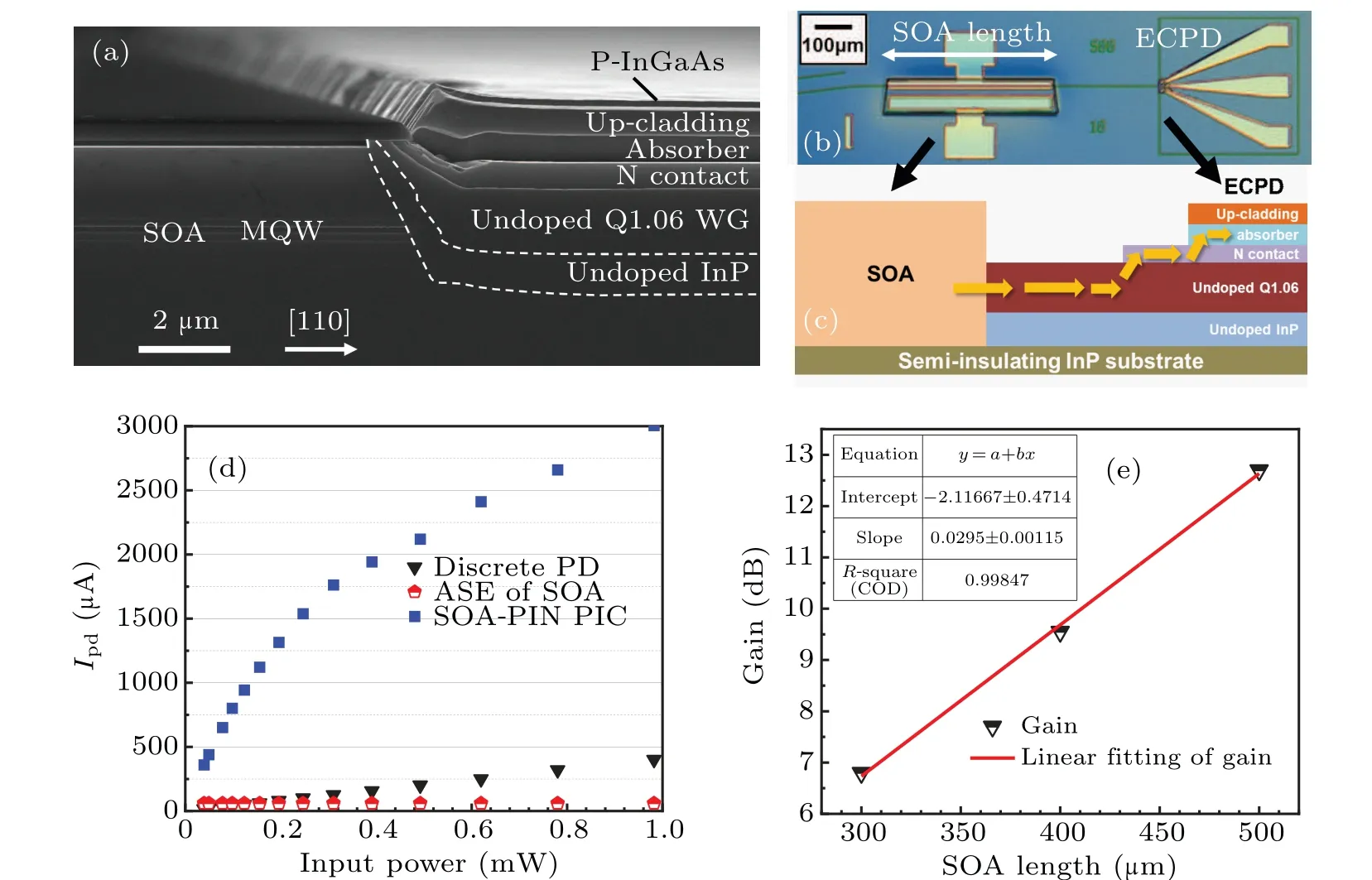
Fig.9. Fabrication results of integrated SOA and ECPD:(a)Regrowth morphology of InP/InGaAsP waveguide and photodetector around butt-joint interface.(b)Photograph of a fabricated SOA-ECPD chip. The SOA is a 2×500μm2 device and the PD size is 5×10μm2. (c)Schematic of ECPD corss section. (d)Photocurrent measurement results at 1545 nm under different input power using a tapered single mode fiber.The injection current density for SOA is 9 kA/cm2.PD is biased at-3 V.(e)Small signal gain versus SOA length and its linear fitting. The injection current density for SOAs is 9 kA/cm2.
Conventional lithography, dry etching and wet etching processes were then used for the fabrication of SOA-ECPD integrated devices. SiO2and photoresist were served as etching mask. SOA and PD are 2×500 μm2and 5×10 μm2,respectively, and they are connected through a 300 μm long waveguide. The passive waveguide is a 2 μm wide shallow ridge waveguide. Figure 9(b) shows an optical photo of the fabricated device.
For ECPD as shown in Fig. 9(c), the light is coupled evanescently from the single-mode Q1.06 waveguide into a multi-mode waveguide,which is composed of n-contact layer and waveguide layer. This stimulates beat effect between multiple modes and produce periodic oscillations in the direction of propagation. By controlling the extended length of the N contact layer, absorber layer at the front end of the PD mesa can contribute to absorption process,improving the responsivity of the detector without affecting the bandwidth.
Figure 9(d) shows photocurrent measurement results of the SOA-ECPD integrated device versus the discrete ECPD.At 9 kA/cm2current density and low input power, the SOAECPD PIC has a responsivity of 7.8 A/W, which is 12.7 dB higher than the 0.4 A/W of discrete ECPD. The small signal on-chip gain of SOA versus device length is plotted in Fig. 9(e). By calculating the intercept of linear fitting curve,the insertion loss of butt-joint interface can be estimated as dB/interface Consequently, we believe that the studied buttjoint regrowth method is qualified for the integration of SOA and ECPD.
4. Conclusion
We have studied butt-joint regrowth of thick passive waveguide layers around deep etched entire SOA mesas,by using low pressure metal-organic chemical vapor-phase epitaxy. By comparing the etching profile of different etchants, we have achieved a non-reentrant mesa profile with smooth side wall by combination of ICP etching and 2HBr:2H3PO4:K2Cr2O7wet etching. A high growth temperature is used to obtain planar regrowth. By comparing the growth morphology and simulating optical transmission along different directions, higher butt-joint coupling efficiency will be obtained along the [110] direction. The relation between growth rate and mask design has been carefully examined and found to provide important guidance for future mask design and photonic integration process. This technology has been successfully employed to realize the integration of evanescent waveguide photodiode and active gain section in a simple way.
Acknowledgements
Project supported by the National Key R&D Program of China (Grant No. 2020YFB1805701), the National Natural Foundation of China (Grant Nos. 61934003, 61635010, and 61674136), and Beijing Natural Science Foundation, China(Grant No.4194093).
猜你喜歡
Chinese Physics B(2023年1期)2023-02-20 13:14:06
科海故事博覽·中旬刊(2022年4期)2022-04-23 16:59:45
中國(guó)應(yīng)急管理科學(xué)(2022年1期)2022-04-18 22:12:38
包裝工程(2022年3期)2022-02-22 10:29:06
電影文學(xué)(2021年17期)2021-11-14 20:46:07
Chinese Physics B(2019年4期)2019-04-13 01:14:24
故事會(huì)(2018年21期)2018-11-05 03:38:50
大眾電視(藍(lán)天下)(2018年7期)2018-10-08 02:12:00
中共南寧市委黨校學(xué)報(bào)(2017年3期)2017-10-21 23:05:00
故事會(huì)(2017年12期)2017-06-22 00:25:46

- Chinese Physics B的其它文章
- Helium bubble formation and evolution in NiMo-Y2O3 alloy under He ion irradiation
- Dynamics and intermittent stochastic stabilization of a rumor spreading model with guidance mechanism in heterogeneous network
- Spectroscopy and scattering matrices with nitrogen atom:Rydberg states and optical oscillator strengths
- Low-overhead fault-tolerant error correction scheme based on quantum stabilizer codes
- Transmembrane transport of multicomponent liposome-nanoparticles into giant vesicles
- Molecular dynamics simulations of A-DNA in bivalent metal ions salt solution