
Thermal stress reduction of GaAs epitaxial growth on V-groove patterned Si substrates*
2021-01-21 02:12:54ZeYuanYang楊澤園JunWang王俊GuoFengWu武國峰YongQingHuang黃永清XiaoMinRen任曉敏HaiMingJi季海銘andShuaiLuo羅帥
Chinese Physics B 2021年1期
Ze-Yuan Yang(楊澤園), Jun Wang(王俊),?, Guo-Feng Wu(武國峰), Yong-Qing Huang(黃永清),Xiao-Min Ren(任曉敏), Hai-Ming Ji(季海銘), and Shuai Luo(羅帥)
1State Key Laboratory of Information Photonics and Optical Communications,Beijing University of Posts and Telecommunications,Beijing 100876,China
2Center of Materials Science and Optoelectronics Engineering,University of Chinese Academy of Sciences,Beijing 100049,China
Keywords: GaAs on Si,thermal stress,V-groove,finite-element method
1. Introduction
Silicon (Si) is a fundamental material of modern electronic technology, and about 95% of all semiconductor devices are manufactured by using Si substrates.[1]But, the physical properties of Si limit its application to optoelectronic devices. Gallium arsenide(GaAs)is a matured secondgeneration semiconductor material with the direct bandgap structure and high electron mobility, which is a favorable optoelectronic material. The quality of GaAs layers directly affects the performances of GaAs optoelectronic devices. The research of directly epitaxial GaAs on Si substrates can combine the matured Si-based integrated circuit process with excellent GaAs-based optoelectronic devices to realize Si-based optoelectronic integration. In addition, the GaAs-on-Si substrate will have a high market potential,which is the basis for manufacturing many kinds of optoelectronic devices, such as lasers,[2,3]solar cells,[4]and photodetectors.[5]
However, obtaining high crystal quality GaAs on Si is still a challenge because of a high density of threading dislocations generated by 4% lattice mismatch and 119% thermal expansion coefficient(TEC)mismatch,anti-phase boundaries (APBs) formation as a consequence of the polar GaAs grown on nonpolar Si system. Many upwardly propagated threading dislocations appear in the GaAs layer.In order to inhibit the threading dislocations from upward propagating,several approaches have been employed for the epitaxial growth,such as two-step or three-step growth method,[6,7]thermal cycles annealing,[8]quantum dots dislocation filters,[9]strained layer superlattice buffer layers,[10]graded buffer layers,[11]and amorphous Si buffer layer.[12]These methods are used individually to grow the epitaxial layer, still resulting in high dislocation density. This is why two or three of these methods are commonly used together in GaAs/Si epitaxial growth.The dislocation density of the GaAs/Si epitaxial layer has decreased to about 105-cm-2orders of magnitude.[13]Nevertheless,these methods need to be less time-consuming before being employed in an industrial manufacturing process.
An alternative approach is to use a nanopatterned Si substrate with SiO2as a mask.[14,15]The method enables the epitaxial layer to realize area-selective growth on the substrate,since forming the nuclei of deposited material on the Si surface requires much lesser free energy than that required on the mask surface. With the development of etching technology,the technology for fabricating nanoscale patterned substrates is becoming more and more matured and cheaper. Moreover,one found that for patterned substrates, the V-groove has its unique advantages in the geometry of kinds of trenches.[16]First,for 60?threading dislocations generated in the course of growth,they tend to glide along the{111}planes.These dislocations will be annihilated on the SiO2mask wall and confined in the trench. The GaAs nucleation on Si(111)generates less defects than the on Si(001).[17]Second,a GaAs lattice in the V-shape of Si with {111} facets is along the [110] direction.The crystallography analysis indicates[18]that GaAs grown on the Si(111)surface cannot result in the formation of APBs in the GaAs layer. Moreover, Li et al. have grown high-quality GaAs films with low dislocation densities through V-groove nanopatterned Si substrates.[19]High-quality GaAs films are conducive to our realizing the fabrication of subsequent devices.
Generally speaking,during the growth of GaAs/Si materials, the lattice stress caused by lattice mismatch is released through dislocations. Subsequently, after epitaxial growth of GaAs on Si substrate is completed,in the cooling process from the growth temperature to room temperature, thermal stress arises due to the difference in TEC between GaAs and Si.When the stress(tensile in GaAs)is sufficiently large, cracks are formed on the GaAs film.[20]The presence of cracks in GaAs thin film is not desirable for device fabrication because they can deteriorate the performance and lifetime of devices fabricated on the epilayers. Therefore, the thermal mismatch effects must be addressed during GaAs epitaxial growth.Thermal stress caused by TEC mismatch has attracted the attention of researchers. Many experiments have confirmed that the thermal stress is existent and harmful.[21,22]Moreover,Li et al. have proved through the photoluminescence spectroscopy that the method of selective area growth of GaAs in V-grooved Si can efficiently relax the strain induced by the TEC mismatch.[23]However, the thermal stress distributed at each point of the structure cannot be measured experimentally.To date, the thermal stress distribution on the GaAs epitaxial layer of V-grooved patterned Si substrates has not been studied in detail. Therefore, in order to fabricate optoelectronic devices with better performance, it is necessary to explore the thermal stress distribution in nanoscale V-groove patterned structures for the growth of GaAs/Si.
In this paper, we aim to systematically study the thermal stress in the coalesced GaAs layer grown on V-groove nanopatterned Si substrate by the finite-element method.First,we describe two models of two-dimensional (2D) structures with GaAs epitaxial growth on planar Si substrate and Vgroove patterned Si substrate, respectively. Subsequently, we compare the thermal stresses of the GaAs layers grown on two kinds of Si substrates. Comparing with the planar Si substrate,the thermal stress is significantly reduced for the GaAs layer on the V-groove patterned Si substrate. Finally,the influences of the width of the V-groove,the thickness and the width of the SiO2mask of the structure on thermal stress of the GaAs epitaxial layer are discussed.The results demonstrate that the role of the SiO2mask and the V-groove are outstanding,reducing the thermal stress on the GaAs layer.
2. Material structures and simulation model
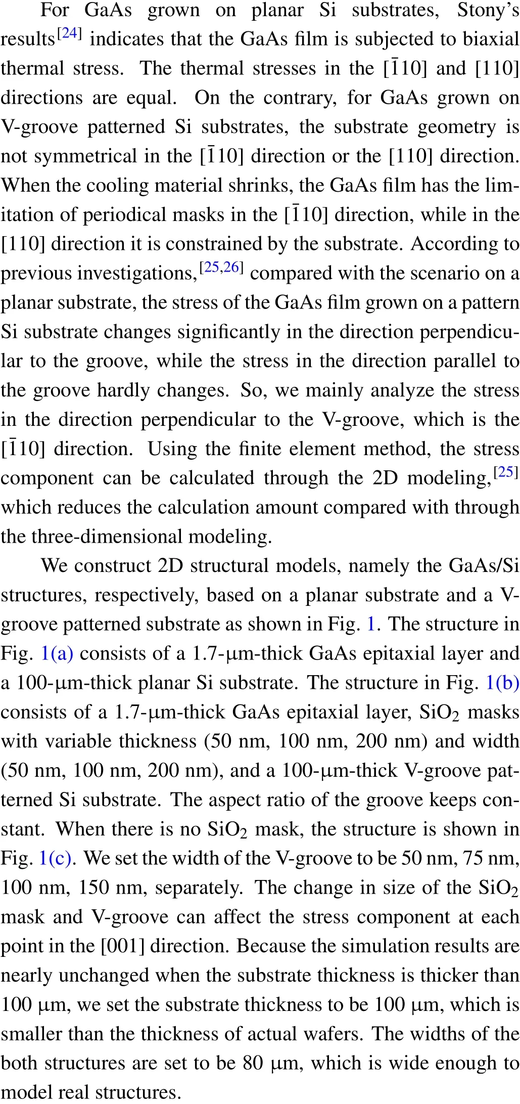
The finite element method is used to calculate the thermal stress distributions of the two structures. The fixed constraint is applied to point O as shown in Fig.1,and the prescribed displacement in the[001]direction is applied to the point O1. All other points in the two structures can move freely according to the law of thermal expansion without any external mechanical constraint. The material parameters are listed in Table 1. The triangular mesh is used to divide the two structures based on geometric dimensions. The extremely fine mesh with a maximum element size of 5 nm and minimum element size of 1 nm is introduced into the model for the GaAs window area and the SiO2mask. For other parts of the mesh,the fine mesh with a maximum element size of 2 μm and minimum element size of 10 nm is used. Experiments have shown that a GaAs epitaxial layer grown at a higher temperature (>650?C) can form a single-crystal layer with better crystal quality.[6]Therefore,for the two GaAs/Si models,it is assumed that they are cooled from the growth temperature of 685?C to room temperature 20?C, and the stability of GaAs thermal stress is analyzed.The effects of the width of the V-groove,the thickness and the width of the SiO2mask on the thermal stress of the structures are investigated.
Fig.1. Structure of GaAs epitaxially grown on(a)planar Si substrate and[(b)and(c)]V-groove patterned Si substrate.
Table 1. Material parameters used in simulations.
3. Results and discussion
The thermal stress distributions of the two 2D models in Fig.1 are shown in Fig.2.Figure 2(a)shows the thermal stress distribution of the structure on the planar Si substrate. It can be seen that the Si substrate is subjected to compressive stress(negative) and the GaAs layer is subjected to tensile stress(positive). At the GaAs/Si interface, the stress has a sharp change. The stress is laterally uniform but it varies with the position of the structure along the z-axis direction. Figure 2(b)shows the thermal stress distribution of the structure on the Vgroove patterned Si substrate. In the structure, the width of the V-groove,the thickness and width of the SiO2mask are all set to be 100 nm. The thermal stress of the structure changes periodically in the lateral direction,and the stress distribution is not uniform at different positions along the z-axis direction,especially near the GaAs/Si interface. Since the TEC of GaAs is much larger than that of Si, the GaAs layer is mostly subjected to tensile stress and the Si substrate is mostly subjected to compressive stress. Near the GaAs/Si interface, the stress may appear in the opposite state of stress. Introducing the SiO2mask,the thermal stress of GaAs layers between masks is significantly reduced. This is because the TEC of SiO2is very small(about 1/11 of GaAs),which hinders the pattern region of GaAs from shrinking in the cooling process. The Si substrate is much thicker than the SiO2mask,so the stress of the GaAs layer away from SiO2masks is mainly determined by the Si substrate. The area influenced by the SiO2mask is only in the window area as shown in Fig.2(b). The maximum stress can reach 339 MPa,which appears in the upper area of the SiO2mask, suggesting that cracks and defects are most likely to occur in the region during the experiment. However,for the small region above the SiO2mask, the cracks and defects can be easy to be avoided by experimental methods,such as forming a gap in the small region.[25]The stress at the bottom of the V-groove(point A)is 209 MPa. Figure 2(c)shows the thermal stress distribution of the structure on the V-groove patterned Si substrate without SiO2mask.Comparing with the planar Si substrate,the thermal stress is reduced for the GaAs layer in the groove. After adding the SiO2mask, the stress reduction is more obvious.
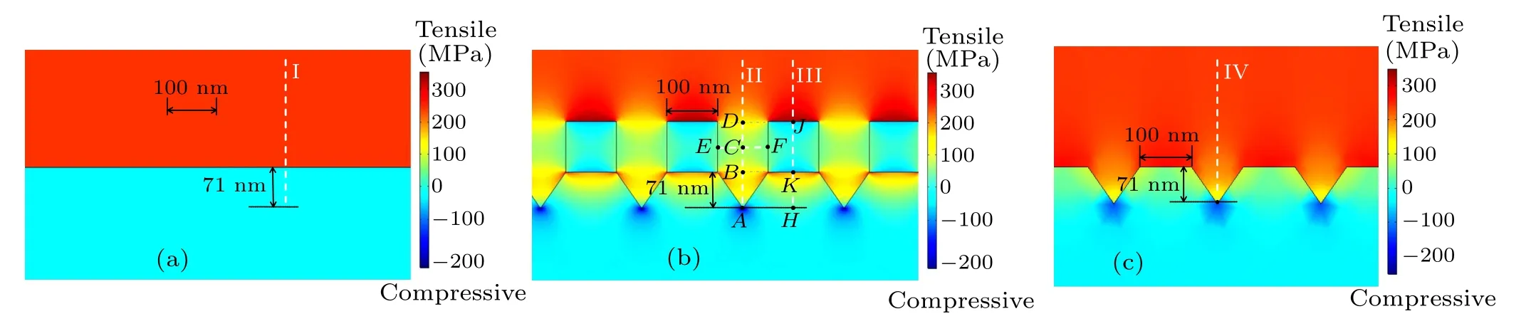
Fig.2. Thermal stress distribution of GaAs epitaxially grown on(a)planar Si substrate and[(b)and(c)]V-groove patterned Si substrate.
Figure 3 shows the thermal stress value along lines I, II,III, and IV in Fig. 2. Line I reveals the thermal stress distribution of the structure on the planar Si substrate. As the distance from the GaAs/Si interface increases, the stress decreases linearly for the Si substrate and the GaAs layer. It is worth noting that the stress changes extremely small within the Si layer and the GaAs layer, separately. The results show that when the distance from the interface is within 71 nm,the compressive stress in the Si substrate is about 32 MPa,and the tensile stress in the entire GaAs layer is about 245 MPa. Line II reveals the thermal stress distribution of the structure on the V-groove patterned Si substrate. As can be seen from line II,near the Si/GaAs interface, the stress of the curve fluctuates greatly in the Si layer and GaAs layer, separately. The GaAs layer is subjected to compressive stress within 5 nm from point A. Then,the GaAs layer is subjected to tensile stress at a distance of more than 5 nm from point A. In addition,the farther away from point A, the smaller the change in stress is, and the final stress is about 244 MPa. Comparing with the planar Si substrate, the thermal stress significantly decreases for the GaAs layer, of which the thickness is within 300 nm on the V-groove patterned Si substrate, and particularly, the average stress of line BD is 100 MPa,which is reduced by 59%. Line III reveals the thermal stress distribution in and around a SiO2mask layer on the patterned Si substrate. The stress of line KJ represents the stress in the SiO2mask layer. A small part of the center in the SiO2mask layer presents the tensile stress,and the rest the compressive stress. And at the edge of the SiO2mask there appears the largest compressive stress. The stresses of line HK and above point J represent the stresses in the Si substrate and the GaAs layer. It can be seen that the closer to the SiO2mask,the greater the tensile stress they are subjected to. Line IV reveals the thermal stress distribution of the GaAs layer on the V-groove patterned Si substrate without SiO2mask. The farther from the bottom of the V-groove,the higher the stress. Obviously, the stress of the structure with SiO2mask is less than that without SiO2mask. In addition,the final stress of the GaAs layer is about 244 MPa. Therefore,the SiO2mask affects the quality of the GaAs in the relevant regions. Finally,it is important to point out that the final stresses of the three lines are close to each other Our results support the experimental results[23]that epitaxial growth on a nanopatterned substrate can effectively release stress due to thermal mismatch.
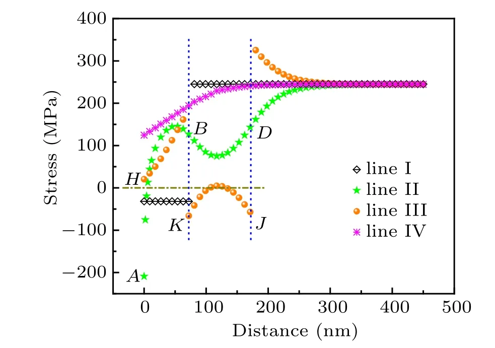
Fig.3. Thermal stress value varying with distance along four lines(lines I,II,III,and IV)in Fig.2.
From the above analysis,we find that the stress in the window area is lower than in other areas, which is more suitable for fabricating optoelectronic devices. Therefore, in the following,we will study the thermal stress values in the window area for different widths of the V-groove,thickness values,and widths of the SiO2mask.
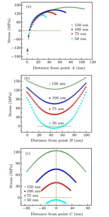
Fig.4. Calculated thermal stress values along(a)line AB,(b)line BD,and(c)line EF for different widths of V-groove,with SiO2 mask being 100 nm both in thickness and in width.
Figure 4 shows the effect of the width of V-groove on the thermal stress. The thermal stresses along lines AB, BD,and EF are shown in Figs. 4(a)–4(c), respectively. We can observe from Fig. 4(a) that the beginning of each curve located at the bottom of the V-groove presents the compressive stress. The compressive stress decreases as the distance increases from point A. This is because the region at the bottom of the V-groove is extremely narrow,and the narrower the GaAs window region,the greater the thermal stress of GaAs in the pattern region is affected by the SiO2mask. We can notice that there is a critical point where the stress is zero. Then the stress is converted into tensile stress on line AB. And the tensile stress on each curve first increases and then decreases as the distance increases from point A. In addition,as the width of the V-groove increases, the maximum of tensile stress increases. It can be seen from Fig.4(b)that the tensile stress on line BD is large at both ends and small in the middle. While the tensile stress on line EF is small at the ends and large in the middle as shown in Fig. 4(c). Due to the symmetry and repeatability of the structure,the stress value of lines EC and FC are the same. Furthermore, the tensile stress of lines BD and EF increase with the width of V-groove increasing. And the wider the V-groove,the more uniform the stress of line BD is.In particular,the stress state at point C is compressive when the width of the V-groove width is 50 nm.
We calculate the average stress in the growth window area of the GaAs layer by the data on lines BD and EF. The result shows that when the width of V-groove is 50 nm,75 nm,100 nm,150 nm,the average stress of the GaAs epitaxial layer in the growth window region is 24 MPa, 53 MPa, 80 MPa,117 MPa,separately
Figure 5 shows the average thermal stress values along line BD and line EF with different thickness values and widths of the SiO2mask, when the width of the V-groove is fixed at 50 nm. As shown in Fig. 5, the size of the SiO2mask has a certain effect on the stress of the GaAs layer. And within a certain range, as the thickness or width of the SiO2mask increases, the average thermal stress first decreases and then increases. When the thickness and width of the SiO2mask are both 100 nm,the average stress is minimum,which is 24 MPa.In Fig.5,the minimum value is clearly marked in gray. In this optimal structure,the aspect ratio of the window area is 2.
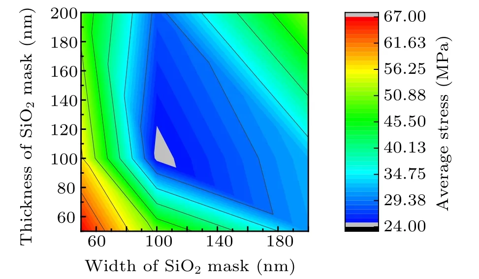
Fig.5. Average thermal stress values along line BD and line EF with different thickness values and widths of SiO2 mask,with width of V-groove being 50 nm.
Table 2 shows the influences of the thickness and width of the SiO2mask in a range of between 0 nm and 50 nm on the average thermal stress of GaAs in the patterned area. Without SiO2mask, the stress is 210 MPa. It can be clearly seen that the introduction of the SiO2mask reduces the thermal stress of GaAs in the patterned area.
So, the three structure parameters that are the width of the V-groove, the thickness and the width of the SiO2mask,significantly affect the thermal stress of the GaAs layer. When the width of V-groove is 50 nm and the width and the thickness of the SiO2mask are both 100 nm, the GaAs layer exhibits a minimum stress. Comparing with the planar Si substrate,the average stress of the GaAs epitaxial layer in the growth window region of the V-grooved Si substrate is reduced by 90%. Finally,Guo et al. demonstrated that high quality GaAs can be obtained in sub-50-nm wide V-groove according to the experiment,[15]so the 50-nm V-groove of our optimal structure is achievable. Li et al.[23]and Freundlich et al.[27]also proved that the method of selective area growth of GaAs on V-grooved pattered Si substrate with SiO2mask can efficiently relax the strain induced by the thermal mismatch,which is consistent with our results. Therefore, our optimal structure can achieve high-quality GaAs growth.
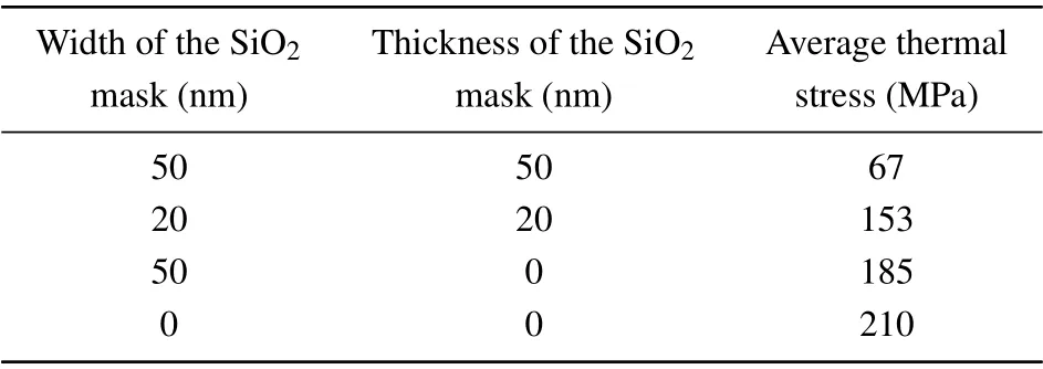
Table 2. Average thermal stress with width of V-groove being 50 nm.
4. Conclusions
In this work we perform the thermal stress analysis of a GaAs layer grown on the V-groove patterned Si substrate by the finite-element method. First, structures of the GaAs layers respectively grown on the V-groove patterned Si substrate and the planar Si substrate are modeled to calculate their stress distributions The results show that the thermal stress distribution near the interface in the patterned substrate is nonuniform,which is different from the planar structure. Comparing with the planar substrate,the thermal stress of the GaAs layer on the patterned substrate is significantly reduced, especially when the thickness of the GaAs layer is within 300 nm. Second,the three factors that are the width of the V-groove,the thickness and the width of the SiO2mask are also studied,which significantly affect the thermal stress distribution of the GaAs layer.The results indicate that when the width of V-groove is 50 nm and the width and the thickness of the SiO2mask are both 100 nm,the GaAs layer is subjected to the minimum stress. In addition, comparing with the planar Si substrate, the average stress of the GaAs epitaxial layer in the growth window region of the V-grooved Si substrate is reduced by 90%. These findings are important for growing the high-quality GaAs films and provide an important step towards the optoelectronic device integration on GaAs substrates.
猜你喜歡
青年文學(xué)家(2024年23期)2024-12-31 00:00:00
Chinese Physics B(2023年12期)2023-12-15 11:51:28
嶺南音樂(2022年6期)2022-02-04 13:50:24
Chinese Physics B(2021年7期)2021-07-30 07:37:30
東坡赤壁詩詞(2020年3期)2020-07-04 02:50:05
黃河之聲(2019年17期)2019-10-21 01:40:38
高中生學(xué)習(xí)·高二版(2016年5期)2016-05-14 20:12:19
Journal of Meteorological Research(2015年5期)2015-11-21 11:23:28
中國衛(wèi)生(2014年2期)2014-11-12 13:00:02
Nuclear Science and Techniques(2014年5期)2014-08-05 09:13:16
- Chinese Physics B的其它文章
- Numerical simulation on ionic wind in circular channels*
- Interaction properties of solitons for a couple of nonlinear evolution equations
- Enhancement of multiatom non-classical correlations and quantum state transfer in atom–cavity–fiber system*
- Protein–protein docking with interface residue restraints*
- Effect of interaction between loop bases and ions on stability of G-quadruplex DNA*
- Retrieval of multiple scattering contrast from x-ray analyzer-based imaging*