
Wafer map defect patterns classification based on a lightweight network and data augmentation
2023-12-01 10:43:02NaigongYuHuaishengChenQiaoXuMohammadMehediHasanOuattaraSie
Naigong Yu| Huaisheng Chen | Qiao Xu |Mohammad Mehedi Hasan | Ouattara Sie,4
1Faculty of Information Technology,Beijing University of Technology,Beijing,China
2Beijing Key Laboratory of Computational Intelligence and Intelligent System,Beijing,China
3Engineering Research Center of Digital Community,Ministry of Education,Beijing,China
4College of Robotic,Université Félix Houphou?t-Boigny,Abidjan, C?te d'Ivoire
Abstract Accurately identifying defect patterns in wafer maps can help engineers find abnormal failure factors in production lines.During the wafer testing stage,deep learning methods are widely used in wafer defect detection due to their powerful feature extraction capabilities.However, most of the current wafer defect patterns classification models have high complexity and slow detection speed,which are difficult to apply in the actual wafer production process.In addition, there is a data imbalance in the wafer dataset that seriously affects the training results of the model.To reduce the complexity of the deep model without affecting the wafer feature expression, this paper adjusts the structure of the dense block in the PeleeNet network and proposes a lightweight network WMPeleeNet based on the PeleeNet module.In addition, to reduce the impact of data imbalance on model training, this paper proposes a wafer data augmentation method based on a convolutional autoencoder by adding random Gaussian noise to the hidden layer.The method proposed in this paper has an average accuracy of 95.4%on the WM-811K wafer dataset with only 173.643 KB of the parameters and 316.194 M of FLOPs,and takes only 22.99 s to detect 1000 wafer pictures.Compared with the original PeleeNet network without optimization, the number of parameters and FLOPs are reduced by 92.68% and 58.85%, respectively.Data augmentation on the minority class wafer map improves the average classification accuracy by 1.8% on the WM-811K dataset.At the same time, the recognition accuracy of minority classes such as Scratch pattern and Donut pattern are significantly improved.
K E Y W O R D S convolutional autoencoder, lightweight network, wafer defect detection
1 | INTRODUCTION
Wafer manufacturing requires a complex process, in which wafer testing and analysis are indispensable.During detection,the staff uses a probe test bench to detect the electrical characteristics of the chip dies and mark the chip dies in different colours on the wafer map according to the quality level.An analysis of the wafer map is helpful for quality control and process evaluation in the semiconductor manufacturing process.
A wafer map contains information on various defect patterns on the wafer surface.For example,the centre pattern may be caused by nonuniformity problems in chemical mechanical polishing(CMP).Scratch patterns may be caused by scratching during material transportation or the mechanical polishing process [1].Therefore, accurately identifying various defect patterns in the wafer map can help engineers find abnormal faults in the production line, improve the efficiency of integrated circuit production, and reduce the rejection rate.In recent decades, the semiconductor industry has developed rapidly under the impetus of Moore's law.The volume of transistors is decreasing,and the technology is becoming more complicated.With an iterative update of the production process, wafer defect pattern detection has changed from manual analysis to automatic analysis of embedded devices with higher efficiency.During the industry's early days, there was a lack of wafer data collection, accumulation, and labelling, so researchers tended to use unsupervised learning methods to study wafer defect pattern detection.With the advent of big data,researchers began to use traditional machine learning and deep learning methods to classify wafer defect patterns.The existing deep learning model has a high classification ability.However, it is difficult to deploy on embedded devices with low computing speed and insufficient storage space because of its large number of parameters and high FLOPs.In addition,there is an extreme data imbalance in each category of wafer defect patterns, which reduces the training effect of the deep learning model.Therefore, realizing a wafer defect patterns classification model with high real-time performance, high classification accuracy, and low complexity is one of the important tasks to identify fault sources and improve yield.
To solve the problem of low detection accuracy and slow speed in the wafer manufacturing process,this paper proposes a lightweight network based on the PeleeNet module and uses a convolutional autoencoder (CAE) to expand the wafer data to solve the wafer map imbalanced data distribution problem.By expanding the wafer map, the generalisation ability of the network is improved.Compared with the traditional deep learning algorithm, the proposed model has higher classification accuracy, lower model complexity, and faster detection speed, which helps to promote the deployment and practical application of the wafer detection model in embedded devices.
The content of this article is organised as follows.The second section discusses the related work of wafer defect patterns classification; the third section elaborates on the lightweight network based on the PeleeNet module and the wafer data augmentation model based on the convolutional autoencoder [2, 3].The fourth section reports a large number of experimental results tested on the WM-811K dataset[4]and the MixedWM38 dataset [5].Finally, the fifth section summarises the research work of this paper and prospects for followup research work.
2 | RELATED WORK
In recent years, researchers have conducted adequate research on the classification of wafer defect patterns, mainly divided into supervised and unsupervised learning.In unsupervised learning, Jin used the density-based spatial clustering of applications with the noise algorithm to cluster the mixed defect patterns of wafers to detect wafer defect patterns of any shape [1].Kim proposed the connected-path filtering method to filter out random defects from the wafer map and adopted an infinite warped mixture model for the clustering of mixedtype defect patterns [6].Yu proposed a local and nonlocal linear discriminant analysis method to extract the characteristics of wafer surface defects and realized the online detection and identification of wafer defects by constructing the corresponding Gaussian mixture model for each defect mode[7].Other unsupervised learning methods including ART [8],K-means [9], and SOM [10], have also been applied to wafer defect pattern recognition.Unsupervised learning can train a model without knowing the class label.The method based on clustering is more flexible for dealing with complex shape defect patterns.It does not need to specify the number of clusters in advance but completes the clustering process simultaneously.When new defect patterns appear, new types of defect patterns can be generalised dynamically by clustering.However, clustering algorithms can only divide the sample space according to the feature distance.
Supervised learning methods usually have excellent classification performance.Wu extracted the radon features and geometric features of the wafer map and realized wafer defect patterns classification through a support vector machine.In addition, similar wafer maps are retrieved by measuring the Euclidean distance of wafer map features, and the WM-811K dataset was published [4].Saqlain proposed an ensemble learning model with multiple weak classifiers for wafer defect patterns recognition[11].Piao extracted the radon feature of a wafer map and classified the wafer map by a decision tree model [12].Through previous studies, it can be found that most wafer defect patterns classifications need to manually extract useful features.In recent years, deep learning has been widely used in the field of image recognition due to its powerful feature extraction ability.Nakazawa trained a convolutional neural network with wafer data generated by simulation and achieved a high classification accuracy on a real wafer dataset.In addition,a convolutional neural network was used to generate the binary code of each wafer map, which realized the retrieval of a similar wafer map [13].Based on depthwise separable convolution and an inverse residual structure, Tsai proposed a lightweight convolutional neural network for wafer defect patterns recognition.This improved the detection speed of the network [14].Jaewoong trained the network through active learning and used less training data to obtain a better classification model[15].Yu proposed a shallow convolutional neural network model for wafer defect patterns detection.By performing dimensionality reduction and similarity sorting on the features extracted by the classification network, the similarity retrieval of wafer images was realized[16].Cheno proposed a CNN model to classify five types of wafer defect patterns.After being combined with the K-NN algorithm, their model can also identify unknown defect patterns [17].Although the method based on deep learning has achieved high accuracy in pattern recognition of wafer defects,most existing models are complex and cannot consider the detection accuracy and speed simultaneously.Hence, this method is not easy to apply in actual industrial production.In the real wafer manufacturing process, the frequency of different faults is different, resulting in a large gap in the number of different types of wafer defects; that is, there is a serious category imbalance.Usually, extreme imbalance of the data distribution seriously affects the learning effect of the deep learning model.To solve this problem, researchers have examined category imbalance in wafer datasets.Hyun used triplet loss and memory mechanisms to classify highly unbalanced wafer datasets in their model [18].Hsu proposed a framework of integrated learning of multiple convolutional neural networks for wafer defect patterns recognition.By setting weights for different classifiers, the impact of category imbalance on the model was reduced [19].To solve the imbalance of wafer categories,many researchers expanded the wafer dataset through data augmentation to achieve the consistency of the number of different wafer maps.Saqlain solved the problem of wafer data imbalance by randomly rotating,clipping, flipping, and other image transformation operations on a wafer map, but randomly clipping the wafer map lost important information [20].Kong Yuting generated more wafer pattern samples through morphological transformation methods, such as corrosion, expansion, open operation, and closed operation, and used rotation and translation operations to simulate the effect of pattern movement[21].However,due to the fixed and regular changes in the size and position of the defect pattern generated by morphological transformation,the morphological richness of the pattern was limited.Wang et al.proposed a data augmentation algorithm AdaBalGAN based on an adaptive GAN for wafer defect pattern generation and recognition, but the complexity of the model is high, and the training process of the GAN model is unstable, with the problems of gradient disappearance and pattern collapse [22].
3 | WAFER DEFECT PATTERN CLASSIFICATION MODEL
The overall scheme proposed in this paper is shown in Figure 1.The method can be divided into two stages: offline modelling and online detection.In the offline modelling stage,a median filter algorithm performs median filter processing on the input image, and the wafer dataset is augmented by the convolutional autoencoder.A lightweight neural network based on the PeleeNet module is built,that can improve the detection speed, reduce the size of the model parameters, and take into account the detection accuracy of the network.In the online detection phase, the same filtering preprocessing operation is performed on the input wafers, and then the wafers to be detected are classified.
3.1 | WM‐PeleeNet model
PeleeNet is a lightweight network variant of DenseNet [23],borrowed from DenseNet's idea of dense connectivity,which is used to address storage and computing power constraints.Unlike a series of lightweight networks such as MobileNet[24,25]and ShuffleNet [26, 27], PeleeNet achieves very good lightweight performance without the use of depthwise separable convolution.This paper prunes the basic structure of PeleeNet and builds a more concise and efficient lightweight network for wafer defect pattern recognition.The lightweight network proposed in this paper is named WM-PeleeNet,and its network structure is shown in Figure 2.This model uses two dense blocks,two transition layers,and one Stem block.
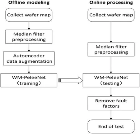
F I G U R E 1 Schematic diagram of overall scheme of wafer defect mode inspection
In addition, before the final global average pooling (GAP)and fully connected layer (FC), a lightweight Convolutional Block Attention Module(CBAM)was added to obtain a more distinguished feature representation.Table 1 lists the detailed parameters and output size of WM-PeleeNet.
3.1.1 | Stem block
The structure of the stem block is shown in Figure 3.Un-like DenseNet, which uses a 7 × 7 convolutional layer with stride of 2 in the first layer,in PeleeNet,a series of small convolution kernels are used.A stem block can integrate features of different scales, thereby effectively improving feature expression capabilities without increasing the additional computational overhead.
3.1.2 | Dense block
Figure 4 shows the internal structure of the dense block,where K is the number of convolution kernels.The dense block is composed of two network branches that capture the receptive fields of different scales.After passing through a Botteneck layer composed of 1×1 convolutional layers,a 3×3 smaller convolution is used for feature extraction to capture the features of small-scale targets.The other method uses two 3× 3 convolutions to learn the visual features of large-scale targets after passing through the bottleneck layer.This is exactly in line with the defect pattern characteristics of the wafer map.For example, the Centre pattern, Loc pattern, and Edge-Ring pattern only occupy a small area of the wafer map, while the Scratch, Donut, and Edge-Ring patterns occupy a larger area of the wafer map.In addition, because the shallow features of the wafer defect pattern map are more important, to extract the shallow features of the wafer map as much as possible while further reducing the computational complexity of the model, this paper adjusts the number of dense layers in the dense block.In the WM-PeleeNet model, there are two dense layers in the first dense layer block and the second dense layer block.In PeleeNet, there is a transition layer between each dense block, and the number of input channels of the transition layer is the same as the number of output channels.We continue this method using a 1×1 convolutional layer and a 2 × 2 average pooling layer as our transition layer.
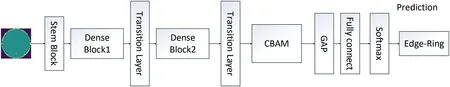
F I G U R E 2 Network structure of WM-Peleenet
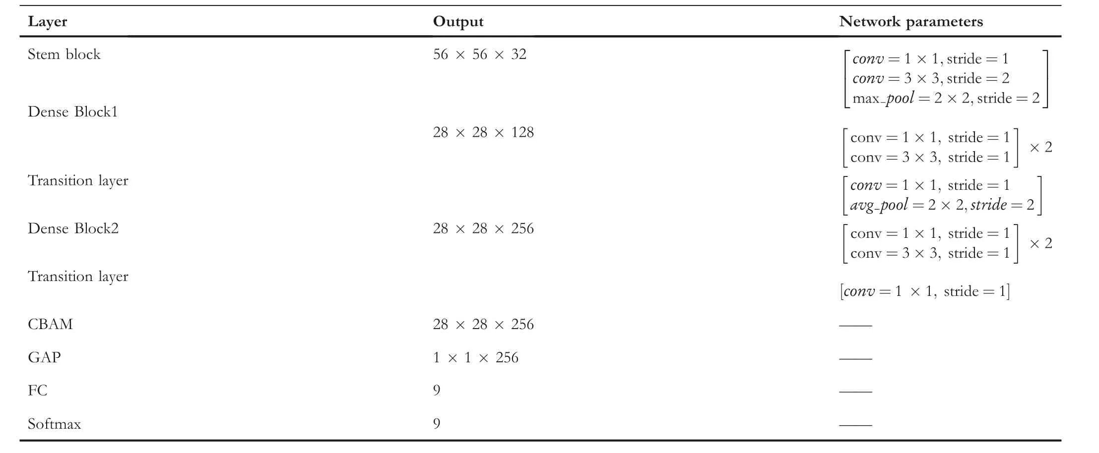
T A B L E 1 Detailed description of WM-PeleeNet

F I G U R E 3 Stem Block of PeleeNet
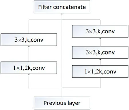
F I G U R E 4 Dense Block of PeleeNet
3.1.3 | Convolutional block attention module
To capture the specific location information of the defect in the wafer map and further improve the classification accuracy of the model, a CBAM is added after the last transition layer.The CBAM module was proposed by Woo et al.in 2018 [30].It is a model that increases the attention mechanism in channel dimensions and spatial dimensions.The CBAM module can generate different weights for the characteristics of each channel and the characteristics of spatial dimensions according to the feedback of the loss function during the training process and enhance the model's ability to extract important information.Since CBAM is a lightweight generalpurpose module, it can be seamlessly integrated into any CNN architecture, and the computational cost is almost negligible.
3.2 | Wafer data augmentation model
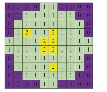
To minimise the impact of data imbalance on model training,a data augmentation method based on a convolutional autoencoder is used to expand the dataset to achieve the relative balance of each category as much as possible.The original wafer map is relatively simple, containing only three types of pixels.The wafer dataset can be augmented by using a simple convolutional autoencoder model.As shown in Figure 5,10×10 raw data are used to generate a wafer map,which is a Centre defect pattern.Among them, 0 stands for the background, 1 stands for normal dies, and 2 stands for defective dies.The autoencoder consists of two main parts:encoder and decoder.The function of the encoder is to encode the highdimensional input X into a low-dimensional hidden variable h, thereby forcing the neural network to learn the most informative features;The function of the decoder is to restore the hidden layer quantity h of the hidden layer to the original dimension.The encoding process of the original data X from the input layer to the hidden layer is shown in (1).The decoding process from the hidden layer to the output layer is shown in (2).
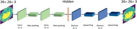
The network structure of the convolutional autoencoder proposed in this paper for wafer data augmentation is shown in Figure 6.In the process of generating the wafer map, this paper first uses a 3 × 3 convolutional layer and a twodimensional maximum pooling layer as an encoder to obtain the potential wafer feature map.Different from the previous autoencoders, after obtaining the potential feature maps, this paper adds Gaussian noise to the potential feature maps to ensure the diversity of the generated wafer maps.The formula for Gaussian noise is shown in(3),whereσis the mean andzis the standard deviation.In the decoder stage, this paper uses a 3 × 3 deconvolution and an upsampling layer to obtain the final generated wafer map.In the generative model proposed in this paper, the loss function is the mean square error of the input image and the output image.The formula is shown in(4).
F I G U R E 5 Raw data for generating a wafer map
4 | EXPERIMENT AND RESULT ANALYSIS
4.1 | Wafer dataset
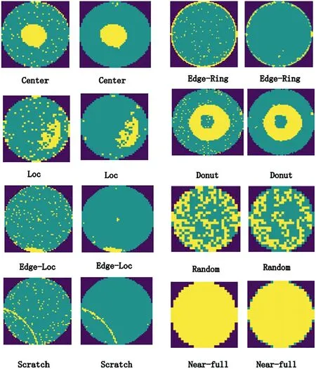
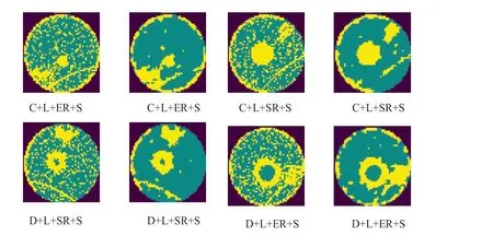
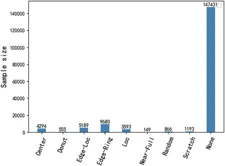
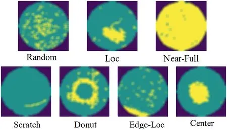
In this paper, we adopt the MixedWM38 and WM-811k datasets to train and test the model.The Mixedwm38 wafer image dataset is generated by simulation, with more than 38,000 wafer images including 8 single defect patterns, 13 mixed defect patterns,12 mixed defect patterns,4 mixed defect patterns,and normal wafers,for a total of 38 kinds.The WM-811K dataset is currently the world's largest publicly accessible wafer map dataset.The dataset was collected during the actual wafer manufacturing process and contains a total of 811,457 wafer images.Among them, 172,950 wafer images have been marked by experts for their corresponding defect types.The WM-811K dataset includes 9 basic wafer modes covering the Centre, Donut, Edge-Loc, Edge-Ring, Loc,Random, Scratch, NearFull, and None patterns.Note that in the 172,950 images marked,None pattern occupies 85.2%,and there is a serious data imbalance.In addition, on the wafer map, there are random defects caused by factors such as the production environment.These defective dies are randomly distributed,do not constitute a specific defect pattern,and are generally regarded as random noise.To eliminate the influence of random defects on the detection accuracy,the median filter algorithm is used to filter the random noise in the two datasets.Except for the None pattern,the wafer map of the WM-811K dataset before and after filtering are shown in Figure 7.Since there are 38 categories in the MixedWM38 wafer dataset,given a limited amount of space, we only show the comparison before and after filtering the wafer map with four mixed defect patterns.This paper uses the first letters of the 8 defect modes to refer to whether there is a certain defect.For example,C+L+SR+S means that there are Centre,Loc,Semi-Ring,and Scratch defects in this wafer map.Figure 8 shows a comparison of the wafer map with four defect patterns before and after median filtering.
F I G U R E 6 Network structure of convolutional autoencoders for wafer data augmentation
F I G U R E 7 Comparison of wafer map before and after filtering in WM-811K dataset (left:original wafer map; right: wafer map after median filtering)
The number of categories in the 172,950 wafer maps marked in the WM-811K wafer dataset is extremely unbalanced, and the None pattern accounts for 85.2%.The distribution of the 9 types of wafer maps marked in the WM-811K dataset is shown in Figure 9.In this paper, the dataset is divided into training,validation,and test sets in a ratio of 60%:15%: 25%.The training set is used to train the model, the validation set is used to adjust and evaluate the model parameters,the test set is used to finally evaluate the performance of the model, and the comparison experiments are performed on the test set.To ensure a relative balance of various types of wafer defect patterns in the training set, this paper first conducts a downsampling operation on the None pattern, and randomly selects 5000 images from the None pattern for training.The number distributions of the wafer map of the training, validation, and test sets are shown in Figure 10.
F I G U R E 8 Comparison of four defect patterns in MixedWM38 before and after filtering
F I G U R E 9 Distribution of nine types of wafer patterns
4.2 | Evaluation indices and training parameters
In the experiment, the average accuracy rate, precision rate,recall rate, and F1 evaluation index are used to evaluate the results of the model classification.The definition of the average accuracy rate is shown in (5).
The calculation formulas for the precision rate and recall rate are shown in (6) and (7).
where accuracy is the average accuracy rate, precision is the precision rate, recall is the recall rate, true positive (TP) is the number of samples with positive samples and positive prediction,true negative(TN)is the number of samples with negative samples and negative prediction, false positive (FP) is the number of samples whose samples are negative but predicted to be positive, and false negative (FN) is the number of samples whose samples are positive but whose predictions are negative.
Sometimes there are contradictions between precision and recall indicators,we need to comprehensively consider the two indicators.Combining the precision rate and recall rate,we can obtain the definition of F1 score, as shown in (8).
In the model training stage, since the Loc pattern and Edge-Loc pattern are only different in the position of the defect, data expansion methods such as random cropping are no longer used.Only by randomly rotating images from the training set to expand the dataset, the input size is 224*224.For the WM-811K dataset,this paper uses 100 batches to train the network,the learning rate is set to 0.0001,and the RAdam optimization algorithm is used to update the network weight parameters.In this experiment, the u and v parameters in the RAdam optimiser are set to 0.9 and 0.999, respectively.Because the WM-811K dataset is collected in the real production process, the data are large, and there are inevitably a small number of false labels.To reduce the impact of these false labels on the prediction results,a label smoothing strategy is used in the model training process to avoid over believing the labels of the training samples.
The experimental hardware uses a Dell T7920 server,64 GB of memory, and dual NVIDIA 2080Ti graphics cards.The software uses the Ubuntu 16.04 system,Python language,and PyTorch deep learning framework.
4.3 | Performance on WM‐811K wafer dataset
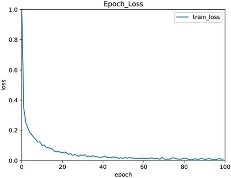
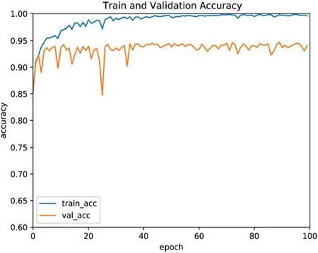
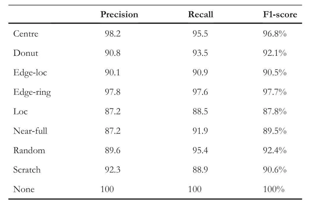
In the WM-881K dataset, the loss value of each round in the training process of 100 epochs is shown in Figure 11.The figure shows that after 60 training batches, the loss curve converges very well.The accuracy curves of the training set and the validation set are shown in Figure 12.As the number of iterations increases,the accuracy of the training set gradually converges to 1,and the accuracy of the validation set gradually converges to 95%.Table 2 shows the classification results of the proposed WM-PeleeNet model for nine wafer patterns.The table shows that for the nine wafer patterns,the proposed model achieved very high precision,recall,and F1 score.In addition,this paper draws a confusion matrix to represent the number of accurate and misclassified defect patterns for all categories.The classification confusion matrix of the 9 wafer patterns is shown in Figure 13.It can be found from the confusion matrix that because the shapes of the two defect patterns of the Edge-Loc patterns and Loc patterns are relatively similar,in the Edge-Loc patterns,3.86%and 3.70%of the samples are mistakenly classified as Edge-Ring and Loc patterns, respectively.In the Loc defect patterns, approximately 7.24% of the Loc pattern samples were mistakenly classified as Edge-Loc patterns.
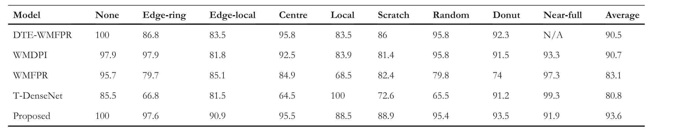
The model proposed in this paper is compared with the wafer defect pattern classification methods of recent years,including DTE-WMFPR (Piao et al.2018) [12], WMDPI(Saqlain et al.2019) [11], WMFPR (Wu et al.2015) [4] , and T-DenseNet (Shen et al.2019) [28].The experimental results are listed in Table 3.The comparison results show that the average classification accuracy of the model proposed in this paper is 93.6% among the 9 wafer patterns, which is better than all other models as a whole.Except for the Scratch and the Loc patterns, the wafer patterns achieved a classification accuracy of greater than 90%.
4.4 | Performance on MixedWM38 wafer dataset
F I G U R E 1 1 Training set loss curve of WM-811K dataset
F I G U R E 1 2 Accuracy change curve of training set and validation set of WM-811K dataset
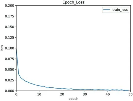
To analyse the convergence and stability of the proposed lightweight network, the changes in the loss value during the training process of the MixedWM38 dataset and the accuracy of the training set and the accuracy of the validation set are examined.For the MixedWM38 dataset, in the process of 50 iterative batches, the curve change graph of the loss function and the accuracy change graph of the training set and the validation set are shown in Figure 14 and Figure 15, respectively.By the 30th round of training, the loss function curve has converged.Table 4 is a comparison between the classification accuracy of the 38 categories of the model in this paper and the classification accuracy of the model proposed by Jiang[29].The average accuracy rate of the lightweight model proposed in this paper is 97.5%, which is much higher than the average accuracy rate of 93.5% of the dataset sharer Jiang.In addition,in the 38 wafer pattern categories,WM-PeleeNet has a higher classification accuracy than Jiang in 31 wafer defect categories.
T A B L E 2 Classification results of wafer defect patterns
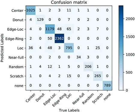
F I G U R E 1 3 Confusion matrix of 9 wafer patterns
4.5 | Wafer map augmentation
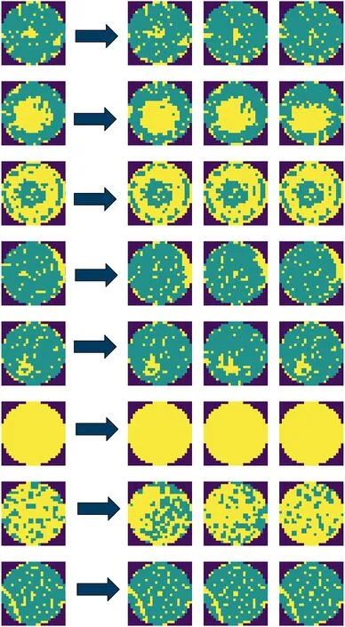
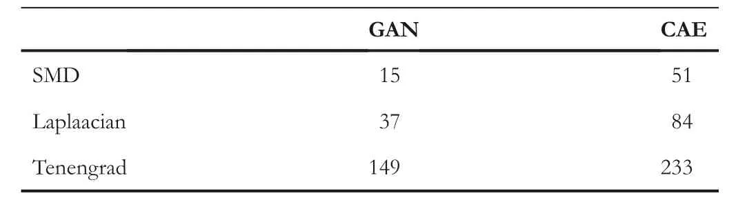
The wafer map generated by the convolutional autoencoder is shown in Figure 16,with the original wafer map on the left and 3 examples of wafer maps generated by the convolutional autoencoder on the right.As seen from Figure 16, the quality of wafer image generated by the convolutional autoencoder is high,and the diversity of wafer defect patterns is increased on the premise of maintaining the original defect cluster pattern.Commonly used data augmentation methods include GANbased image generation methods and image transformationbased methods.The wafer map generated by GAN is shown in Figure 17.The wafer map generated by GAN is rich in defect patterns, but the image is blurry.In the method based on image transformation, this paper uses Gaussian blur,scaling,cropping,rotation,and flipping to augment the training samples.The generated image is shown in Figure 18.
To compare the quality of wafer images generated by convolutional autoencoders and GAN,three indicators of Sumof modulus of grey difference (SMD), Laplacian gradient, and Tenengrad gradient were used to evaluate the definition of the images.For the three evaluation indicators,the larger the value,the higher the definition of the image.To avoid the influence of accidental factors,5000 images were randomly selected from the generated wafer maps, and the average value of the three evaluation indices was calculated as the final quantitative evaluation index.Among the evaluation methods,the quality of samples generated based on convolutional autoencoders is significantly higher than that of images generated based on GAN.A comparison of the three evaluation indicators is shown in Table 5.
T A B L E 3 Comparison with classical wafer map defect pattern classification algorithms (%)
F I G U R E 1 4 Training set loss curve of MixedWM38 dataset

F I G U R E 1 5 Accuracy curve of training set and validation set on MixedWM38 dataset
To further demonstrate the effectiveness of the method proposed in this paper, comparisons are also made with commonly used methods for dealing with data imbalance,including class-balanced sampling and reweighting.In classbalanced sampling, each class is sampled with the same number of samples.Reweighting is achieved by adding a suppressor factor to the cross-entropy loss function.The modified loss function is shown in Equation (9), wherediis the weighting factor representing the proportion of the number of samples in theicategory in the number of samples in all categories, y is the sample label, and ^yis the prediction result.
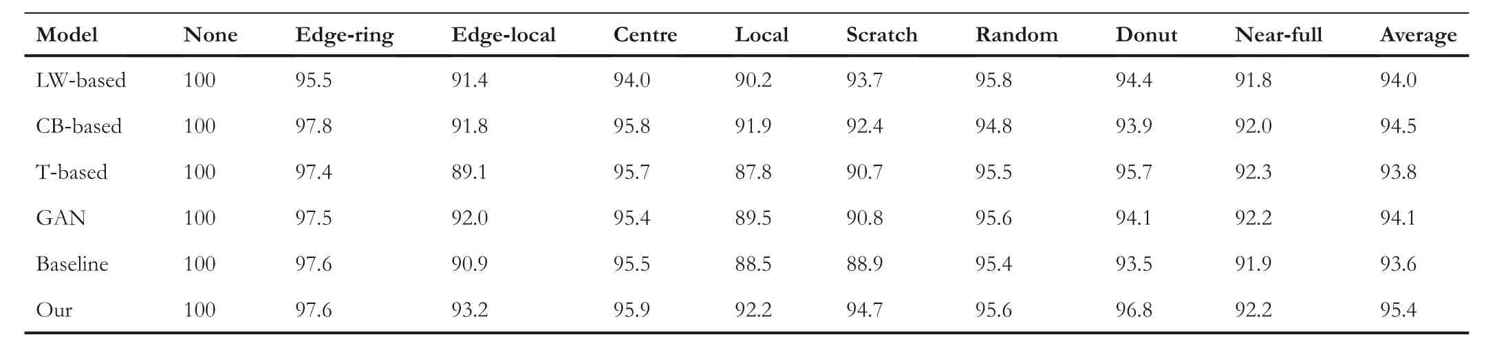
In wafer map data augmentation,we expand the number of wafer maps per class in the training set to 5000 based on the convolutional autoencoder, GAN-based, and image transformation methods,and use the proposed lightweight network for training.Taking the dataset without data augmentation as the baseline, the experimental results are shown in Table 6,where LW-based represents the reweighting method,CB-based represents the class-balanced sampling method, and T-based represents the image transformation method.From Table 6,it can be found that by augmenting the wafer category with a small number of samples in the training set, the average accuracy rate is improved by 1.8%.In addition,the classification accuracy of previous wafer defect pattern categories with fewer categories, such as the Donut and Scratch patterns, is significantly improved.Among them,Donut's classification accuracy increased by 3.3%, and Scratch increased by 5.8%.It can be seen that the wafer data are augmented by the convolutional autoencoder, which reduces the impact of the imbalanced distribution of data categories on model training.
Compared with other methods, the method proposed in this paper exhibits the largest improvement, which is 1.8% higher than the baseline.In contrast, the image transformation-based method has the smallest improvement because the important defect cluster features in the original wafer map are destroyed by cropping, and various image transformation operations have no effect on symmetrical images.The image generated by GAN is relatively blurry.This is equivalent to adding a layer of Gaussian noise to the wafermap, which affects the classification and prediction ability of the model.Compared with the model using the original data,the method based on reweighting only improves the average classification accuracy by 0.4%, and the accuracy of individual categories decreases.The reason is that the weighting of the loss function leads to excessive attention to small samples in the model training process data.The method based on class balanced sampling does not use all of the samples,and it is easy to ignore the samples with representative characteristics.

T A B L E 4 The classification accuracy of each category on MixedWM38 dataset (%)
F I G U R E 1 6 Wafer map generated by convolutional autoencoder
F I G U R E 1 7 Wafer map generated by Generative Adversarial Network
4.6 | Performance of lightweight model
At present, the comparison of the lightweight performance of the model is mainly based on the amount of calculation and the number of parameters, the amount of calculation corresponds to the time complexity, and the number of parameters corresponds to the space complexity.The greater the amount of calculation, the higher the requirements for the CPU or GPU.The higher the number of parameters, the higher the requirements for the chip's video memory.This paper uses the same definition of FLOPs in ResNet [30] to compare the computational complexity of each model; that is, FLOPs are defined as the number of operations of multiplication and addition in the model (multiplication-adds).

F I G U R E 1 8 Augmentation based on image transformation
T A B L E 5 Comparison of generated wafer map quality
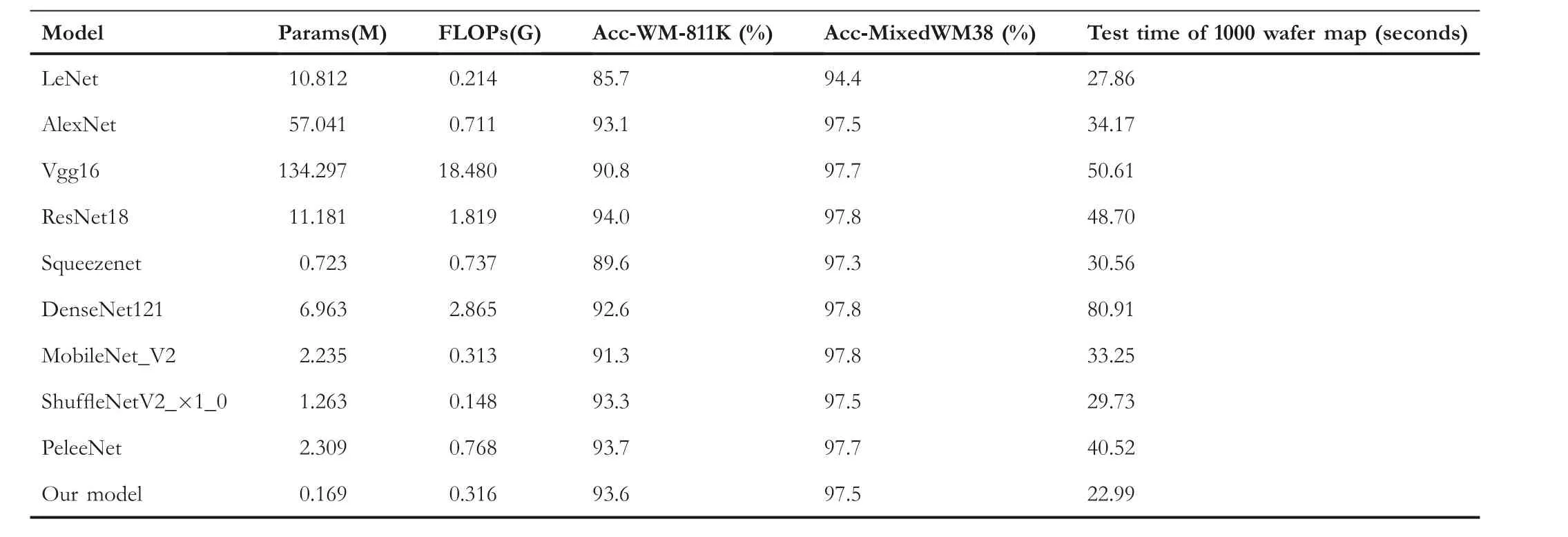
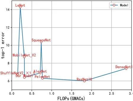
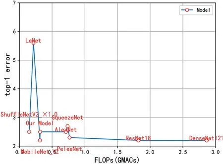
In the experiment of this paper,the size of the input image is set to 224*224 uniformly.In order to avoid the influence of other factors,data augmentation is not performed on the wafer map data in this experiment.The results for the parameters,FLOPs,and average accuracy of different models are shown in Table 7.Figure 19 and Figure 20 show the parameters,FLOPs,and top1-error of different models on the WM-811K dataset.Figure 21 and Figure 22 show the experimental results of the parameters,FLOPs,and top-1 error of different models in the MixedWM38 dataset.
The WM-PeleeNet model proposed in this paper only has 316.194 M FLOPs and 173.643 KB parameters, and the parameters are 1.56%, 0.30%, 0.13%, 1.51%, and 23.37% of LeNet [5], AlexNet [31], VGG16 [32], ResNet18, Denese-Net121, and SqueezeNet [33].FLOPs accounted for only 44.44%, 1.71%, 17.37%, 42.88%, and 11.03% of AlexNet,VGG16, ResNet18, DenseNet121 [34], and SqueezeNet [35],respectively.Compared with the current common lightweight networks MobileNetV2 and ShuffleNetV2_×1_0, the parameter index of WM-PeleeNet proposed in this paper is 7.56%of MobileNetV2 and 13.38% of ShuffleNetV1_1.0, respectively.In terms of the size of FLOPs,the lightweight model proposed in this paper is basically equivalent to MoileNetV2, both of which are more than 300 M, which is approximately twice the size of ShuffleNet V2_×1_0.However, the average accuracy of the WM-PeleeNet network on the WM-811K dataset exceeds that of MobileNetV2 and ShuffleNet V2_×1_0.The average accuracy on the MixedWM38 dataset is basically the same.Compared with the original PeleeNet network without pruning, the number of parameters and FLOPs is reduced by 92.68% and 58.85%, respectively, but the average accuracy rates on the WM-811K dataset and the MixedWM38 dataset are only reduced by 0.1% and 0.2%, respectively.This paper also compares the time taken by the CPU to classify 1000 wafer images.The proposed lightweight model takes only 22.99 s,and the classification accuracy reaches 99.6%,which is much better than the other models.
In general, compared with other models, the lightweight network WM-PeleeNet proposed in this paper has fewer parameters, fewer FLOPs, and higher average classification accuracy.This improves the possibility of deploying deep learning models in the wafer industry.
5 | CONCLUSION
This paper proposed a lightweight network WM-PeleeNet based on the PeleeNet module and augments wafer data through a convolutional autoencoder.Experiments werecarried out on the WM-811K wafer dataset and the MixedWM38 mixed defect wafer dataset.The results showed that the proposed model has faster detection speed and lower model complexity on the premise of losing minimal recognition accuracy.The wafer map generated by the convolutional autoencoder not only maintained the defect characteristics of the original wafer map but also increased the diversity of the wafer map.Compared with the unbalanced dataset,the average classification accuracy improved by 1.8% after data augmentation by the convolutional autoencoder.However, the model in this paper misclassified the Loc and Edge-Loc patterns.In the training process, a large amount of wafer map data is still needed.When a new defective wafer with a small amount of data appears, it cannot be effectively identified.Next, we will focus on the high-precision classification of the Loc and Edge-Loc patterns and how to classify small sample wafer defect maps.
T A B L E 6 Comparison with other imbalanced dataset processing methods (%)
T A B L E 7 Comparison with wafer defect pattern classification models (%)

F I G U R E 1 9 Params and top-1 error of different models on WM-811K dataset
F I G U R E 2 0 FLOPs and top-1 error of different models on WM-811K datasetz
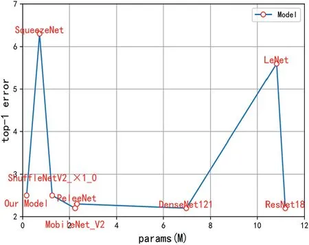
F I G U R E 2 1 Params and top-1 error of different models on MixedWM38 dataset
F I G U R E 2 2 FLOPs and top-1 error of different models on MixedWM38 dataset
ACKNOWLEDGEMENT
This work was supported by a project jointly funded by the Beijing Municipal Education Commission and Municipal Natural Science Foundation under grant KZ202010005004.
CONFLICT OF INTEREST
The authors declare that there is no conflict of interest that could be perceived as prejudicing the impartiality of the research reported.
DATA AVAILABILITY STATEMENT
These data were derived from the following resources available in the public domain: http://mirlab.org/dataSet/public/.
ORCID
Naigong Yuhttps://orcid.org/0000-0002-8452-4623
 CAAI Transactions on Intelligence Technology2023年3期
- CAAI Transactions on Intelligence Technology的其它文章
- Fault diagnosis of rolling bearings with noise signal based on modified kernel principal component analysis and DC-ResNet
- Leveraging hierarchical semantic‐emotional memory in emotional conversation generation
- Forecasting patient demand at urgent care clinics using explainable machine learning
- A federated learning scheme meets dynamic differential privacy
- SRAFE: Siamese Regression Aesthetic Fusion Evaluation for Chinese Calligraphic Copy
- Kernel extreme learning machine‐based general solution to forward kinematics of parallel robots