
Epitaxy of III-nitrides on two-dimensional materials and its applications
2022-11-21 09:29:18YuXu徐俞JianfengWang王建峰BingCao曹冰andKeXu徐科
Chinese Physics B 2022年11期
Yu Xu(徐俞) Jianfeng Wang(王建峰) Bing Cao(曹冰) and Ke Xu(徐科)
1Suzhou Institute of Nano-Tech and Nano-Bionics(SINANO),Chinese Academy of Sciences(CAS),Suzhou 215123,China
2Shenyang National Laboratory for Materials Science,Shenyang 110010,China
3School of Optoelectronic Science and Engineering&Collaborative Innovation Center of Suzhou Nano Science and Technology,Soochow University,Suzhou 215006,China
4Key Laboratory of Advanced Optical Manufacturing Technologies of Jiangsu Province&Key Laboratory of Modern Optical Technologies of Education Ministry of China,Soochow University,Suzhou 215006,China
5Jiangsu Institute of Advanced Semiconductors Ltd,Suzhou 215123,China
III-nitride semiconductor materials have excellent optoelectronic properties, mechanical properties, and chemical stability, which have important applications in the field of optoelectronics and microelectronics. Two-dimensional (2D)materials have been widely focused in recent years due to their peculiar properties. With the property of weak bonding between layers of 2D materials,the growth of III-nitrides on 2D materials has been proposed to solve the mismatch problem caused by heterogeneous epitaxy and to develop substrate stripping techniques to obtain high-quality, low-cost nitride materials for high-quality nitride devices and their extension in the field of flexible devices. In this progress report, the main methods for the preparation of 2D materials,and the recent progress and applications of different techniques for the growth of III-nitrides based on 2D materials are reviewed.
Keywords: nitrides,two-dimensional materials,van der Waals forces
1. Introduction
Epitaxial growth is an important technique for preparing single crystal films, which can be divided into heteroepitaxy and homoepitaxy. Among them,homoepitaxy can obtain high-quality epilayers that match the substrate structure, but production cost is a factor restricting its further development,especially for III-nitrides. At the same time, crystal quality of heteroepitaxy layers is limited by the lattice and thermal mismatch between the epilayer and substrate, which greatly reduces the performance of integrated electronic devices.
In order to reduce generated defects and dislocations during preparation, various epitaxial methods have been developed, such as low-temperature buffer layers,[1,2]and epitaxy lateral over-growth (ELOG).[3]Nevertheless, the quality of the prepared films through heteroepitaxy is different from that through homoepitaxy by several orders of magnitude.
In recent decades, the unique properties of twodimensional (2D) materials and the development of devices based on 2D materials have attracted people’s widespread attentions.[4–7]2D materials refer to the material with only the thickness of the atomic layer in a certain dimension and the other two dimensions with larger scales. The atoms of 2D materials are connected by covalent bonds and the layers of atoms are connected by van der Waals(vdW)forces.[8]
At present, 2D materials are mainly divided into the following types: graphene,[9–14]h-BN,[15–19]transition metal disulfide compounds (TMDCs),[20–24]and others.[25–28]Unlike three-dimensional (3D) materials, 2D materials exhibit unique mechanical, magnetic, thermal, and optical properties due to the small size effect. For example, graphene exhibits high electron mobility,[29,30]high elastic strength,[31]high thermal conductivity,[13]and transparency.[32]The activated graphene can be made into the electrode of supercapacitor, used to store a large amount of charge and energy.[33]H-BN has good electrical insulation and thermal conductivity known as white graphene, usually used in deep ultraviolet (UV) light sources, dielectric layers, cosmetics, microwave transparent shielding layers,etc.[30]On the other hand, the more stable materials in TMDCs are WSe2, MoS2,WS2, and MoSe2, which are direct band gap semiconductor materials with strong spin–orbit coupling and good electronic, mechanical properties. The excellent performance of these 2D materials makes them very attractive applications and development in the field of electronics and optoelectronic devices,[6,34–37]energy conversion and storage,[38–41]catalytic,[42–44]and photodetector.[45–48]
The process of growth thin-film materials on 2D materials is called van der Waals epitaxy(vdWE)and its principle is to use the weak vdW interaction on the surface of the 2D material to connect the epilayer and substrate. Due to the covalent bonding of conventional epitaxy(CE),the lattice mismatch of different materials causes greater strain at the interface and reduces the quality of the material.Unrestricted lattice matching exists on the surface of 2D materials due to the absence of dangling bonds and low surface free energy. Even if existence of large in-plane mismatch,no excessive interface strain exists in quasi-van der Waals epitaxy(QvdWE).
Using 2D materials as the substrate for 3D films growth,the interface between 3D and 2D material exhibits a weaker chemical interaction than the interface between 3D epilayer and 3D substrate,but the interface interaction of the former is stronger than the pure 2D and 2D vdW interaction. Some people also suppose that the epitaxy method of 3D film deposited on 2D material is QvdWE.[49–51]The fly in the ointment is that high-quality single-crystal 2D materials are difficult to obtain,using these 2D materials as substrates will seriously affect the crystallinity of the epilayer. In theory, the weak interfacial forces of the 3D/2D system are helpful in alleviating the large dislocation density associated with the interfacial strain of CE.However,in fact,the low interfacial force is not strong enough for 2D materials to influence the orientation relationship, results in large twist angles occurrence between the initial nucleated grains, which sets the stage for grain boundaries in subsequent film growth.This is the reason why the dislocation density of III-nitride materials grown by QvdWE has remained high so far. Therefore, the 3D films obtained in this way are not conducive to the performance of devices. How to obtain high-quality single-crystal films has become increasingly important.
In 1969, Distler and Shenyavskaya pointed out for the first time in a report that the amorphous intercalation layer in the epitaxy can be used as a channel to transmit direct epitaxial structure information and the epilayer is oriented by the underlying single-crystal substrate.[52]Similarly, Kimet al.obtained a GaAs epilayer with the same orientation as the substrate through single layer graphene (SLG) on a singlecrystal GaAs substrate, they called this method “remote epitaxy(RE)”.[53]At present,it may be a solution to obtain highquality single-crystal films on 2D materials.
Through this technology,it is hoped that a covering layer with the same lattice information can be obtained on any single-crystal substrate with 2D materials. The heterostructures composed of 2D materials are mainly 2D/2D, 3D/2D,and 2D/3D herterostructures. Considering the necessity of studying film growth on 2D materials,we pay more attention to the stacking of 3D/2D heterojunction structure. Whether it is ELOG, QvdWE, or RE, the assembly structure of 2D materials as a buffer layer should have the following advantages:(i) The 2D material insertion layer greatly buffers the interface lattice and thermal mismatches of 3D/2D/3D structures,thus reducing the strain and dislocations. (ii) The weak connection between the epilayer and 2D material can be blocked by, for example, mechanical release, thereby facilitating the peeling and transfer of the epilayer material. (iii) Small size effect brings unique electrical,magnetic,optical,thermal,and mechanical properties to 2D materials,so new 3D/2D assembly structures are bound to change the performance of devices with conventional 3D/3D heterogeneous structures. In the 3D/2D assembly structure, the quality of the material determines the device performance. In order to obtain highquality films and excellent performance heterojunction, we need to understand its competitive growth mechanism and unique physical coupling phenomenon,especially for QvdWE and RE.
In this review, we summarize the methods of III-nitrides grown on 2D materials and 3D/2D integrated devices, with particular emphasis on key technologies for achieving highquality 3D films on 2D materials. In this article, we provide the development progress of this technology according to different extension methods. In the first part,we introduced 3D/2D growth technologies and unique properties by QvdWE.The second part explains how a new technology called RE can achieve high-quality 3D films and device integration characteristics in different fields in order to achieve a wider range of applications.
2. Methods for the preparation of 2D materials
For III-nitrides epitaxy, the 2D materials should accord with the following conditions:
(i) Thermal stability: III-nitrides usually fabricated at high temperature(~800°C for MBE,~1040°C for MOCVD and HVPE).Therefore,2D materials with high thermal stability can be used for III-nitrides epitaxy,such as graphene,BN.TMDCs (such as MoS2or WS2) should be protected before epitaxy.
(ii) Lattice structure: III-nitrides are hexagonal system materials. As a result, hexagonal-honeycomb-structure 2D materials are more suitable for III-nitrides epitaxy. For example,h-BN is more suitable than c-BN.
2.1. Methods of graphene preparation
Graphene was a typical 2D material used for epitaxial growth of III-nitrides,which itself had excellent physical properties and played an important role in devices. The unique 2D structure of graphene could effectively alleviate the lattice mismatch between the epilayer and substrate, and reduced the strain and dislocations during growth. During epitaxial growth, the quality of 3D materials was mainly influenced by 2D materials. The preparation method of largearea and high-quality graphene was a prerequisite. The current graphene preparation methods included micromechanical exfoliation,chemical vapor deposition(CVD),redox,and epitaxial growth. Among them, CVD or SiC epitaxy were the more widely methods for obtaining graphene to epitaxial growth of III-nitrides at present.
In addition, large-area 2D materials fabrication had become mature in industry. For CVD graphene on copper foils,roll-to-roll production of large-area polycrystalline graphene films has begun to be in market after 2010.[54]Wafer-scale singlecrystalline graphene has been realized about 2012.[55]For graphene grown on noncatalytic substrates, wafer-scale singlecrystalline graphene can be fabricated on Ge,[56]SiC,[57]and sapphire[58]substrates, which can be used for epitaxy of III-nitrides directly.
2.1.1. CVD method
CVD method to prepare graphene generally used metals(such as Cu,Ni,and Pt,etc.) as substrates and gaseous hydrocarbons(such as methane,ethylene,etc.) as carbon sources by metal catalysis at high temperatures. The principle was that gaseous substances containing carbon,under high temperature and vacuum, deposited on the surface of substrate, and thus formed a continuous graphene layer.
Since 2009, when Rouffet al.first used CVD to synthesize graphene,[59]this highly controllable and relatively lowcost method for synthesizing high-quality,large-area graphene had been attracted more attentions. The quality of CVD graphene is governed by the substrate,precursors,and growth conditions. The growth conditions of CVD were often harsh because the growth process required high-temperature cleavage of carbon precursors followed by rapid cooling to form graphene. In recent years, many scholars had conducted a lot of researches on these growth factors, and the CVD growth parameters of graphene had been optimized continuously, and now there are some feasible methods to synthesize high-quality graphene films at low temperature,[60]low pressure,[61]and metal-free substrates,[62]which gradually got rid of the constraints of strict growth conditions and expanded the applicability of CVD methods. After the research of our group, we found that the defects of graphene were directly influenced by the growth conditions,and in plasma enhanced chemical vapor deposition (PECVD), the defect type of graphene changed from vacancy to boundary type with the increase of ion source power; the morphology of graphene changed from 2D to 3D with the increase of temperature or ion source power,[63]which was beneficial for us to prepare especial graphene on non-catalytic substrate,such as sapphire,GaN, and AlN substrates. At present, CVD method could achieve large area graphene preparation, which was the most ideal and widespread preparation technique in industrial production.
2.1.2. SiC epitaxial method
The SiC epitaxy method was used to remove Si by heating single crystals of SiC, leaving carbon atoms to undergo reconstruction on the substrate surface to form a graphene layer. The SiC sample obtained by oxygen or hydrogen etching was heated by electron bombardment under high vacuum to remove the oxide, and then the sample was heated to 1250°C–1450°C and heat preservation for 1 min–20 min to obtain a graphene layer. This method usually produced single-crystal graphene as the epitaxial graphene, the orientation relationship of graphene and SiC was considered as[1-100]graphene‖[11-20]SiC. However,it was difficult to prepare large-area graphene with a single layer.
The advantages of SiC-prepared graphene were that the graphene films could be epitaxially grown on commercial SiC substrates, which were now commercially available in large size, and that the grown graphene could be patterned using standard etching techniques with no transfer process involved,making the technology compatible with current semiconductor technologies. Moreover, it has also been proposed in the literature that the epitaxial graphene structure and electronic properties could be tuned by nitrogen ion injection.[64]The graphene obtained by the SiC epitaxial method was very clean and free of contamination or defects from transfer, and could be directly applied to device preparation. However,due to the expensive price of the SiC substrate and the high temperature required for epitaxial preparation, the cost of graphene prepared by SiC epitaxy was expensive.
2.2. Other methods of preparing 2D materials
Mechanical stripping was first reported in 2004 as a method for producing monolayers of graphene. This method was to use tape to repeatedly adhere block layer graphite,gradually thin layer graphite. When it reached a certain level, the ultrathin graphene nanosheet was transferred to the substrate by pressing and heating. The substrate has a reflective effect,so that the graphene nanosheet could be clearly observed under an optical microscope. The 2D materials obtained by this method have the disadvantages of small size,disuniform morphology and thickness and low film yield. However,it is still an important method for preparing 2D semiconductor materials due to its low cost and availability.
Besides graphene, there are many 2D materials, such as h-BN,black scale,silicene,and germanene,etc.[65]These 2D materials have excellent optical, mechanical, thermal, magnetic, and other properties. By stacking different types of 2D materials, a more functional material system can be constructed. Therefore,these materials are expected to find applications in high-performance electronic devices,optoelectronic devices, spintronic devices, and energy conversion and storage.
This section mainly introduces the preparation methods of h-BN and other 2D materials, including mechanical stripping CVD,molecular beam epitaxy(MBE),liquid phase stripping,and wet chemical synthesis.
CVD is a bottom-up growth method, which has the advantages of relatively simple and diverse precursors, good growth speed,etc.[66]CVD can be used to fabricate 2D materials with a large area,but the preparation process of different materials is very different,and it is difficult to control the number of layers. Among them, metal–organic chemical deposition (MOCVD) can accurately and repeatability grow from a single atomic layer to a thick epitaxy layer. This method can be used to grow various V main group and subgroup compound semiconductors and their multiple solid solution thin layer single-crystal materials. For example,many teams have successfully demonstrated the growth of h-BN epitaxy layer by MOCVD.
MBE is a single-crystalline growth technology for highquality crystals film. This method can be used to prepare single-element 2D materials,such as silicone,germanene;and dual-element 2D materials,such as h-BN,MoS2,etc.Its main advantage is that it can be implemented in ultra-high vacuum conditions for accurate control of growth parameters. MBE method is also characterized by extremely slow growth rate,which is also conducive to achieving accurate control of thickness structure and composition.[67]
The liquid phase stripping method is simple and convenient for large-scale preparation of 2D materials. This method can be used for large-scale preparation of antimonene,[68]which has broad application prospects in industrial production. However, due to the introduction of defects and liquid phase contamination in the preparation process, the intrinsic properties of 2D materials will be affected to a certain extent.
Wet chemical synthesis can produce high-quality ultrathin 2D materials. Wet chemistry is a method of synthesis of certain precursors in solution which depends on biochemical reactions under suitable experimental conditions.This method has strong controllability and is a convenient and renewable method for preparing ultra-thin 2D materials. This method can use various ligands to synthesize 2D metal nanomaterials with different sizes and morphologies,crystal phases,and thicknesses. It has great potential in the application of mass synthesis of 2D metal nanomaterials.
3. Epitaxial growth of III-nitrides on 2D materials
3.1. QvdWE
Since Komaet al.first demonstrated the Se/Te and NbSe2/MoS2material systems in 1984,[69]vdWE has proven to be a highly advantageous heterogeneous epitaxy route.VdWE is also a way to grow film materials on substrates,with the difference that the epitaxial and substrate layers are bonded together by weak vdW forces. In the QvdWE process of IIInitride materials, multilayers of 2D materials are introduced between the epilayer and substrate layer to take advantage of the lack of suspended bonds on the surface of the 2D materials,so that the epilayer interacts with the 2D materials only through weak vdW forces. The lattice arrangement of the epilayer at the initial growth stage is not strict match to that of 2D materials,but maintains its own intrinsic lattice parameters,so that the lattice constants are very close to those of the bulk material,with almost no strain residues.
The application of QvdWE in heterogeneous epitaxy relaxes the lattice mismatch and thermal mismatch requirements between the epilayer and substrate layers and the weaker vdW forces between the epilayer and underlying substrate layer make it easier to peel the epitaxial film. In 2010, Chunget al.had published an article inScienceto apply graphene for the epitaxial growth of GaN,[70]which achieved the transfer of GaN films with the help of the layered structure of graphene substrate. In 2018, Ouet al.grew high-quality, low-strain monocrystalline AlN films on WS2/sapphire substrates using MOCVD technology,providing a potential solution for further development of deep ultraviolet light emitting diodes (DUV LEDs)on unconventional substrates.[71]In recent years,there has also been a major breakthrough in the synthesis of IIInitrides on amorphous substrates. Liuet al.synthesized quasisingle-crystalline GaN films on amorphous glass substrates with GaN nanopillars as a buffer layer on graphene, verifying that QvdWE can break through the substrate limitations to achieve III-nitrides growth on amorphous substrates.[72]
Our group has been studying the growth of III-nitrides on graphene by QvdWE in recent years. In 2017, Xuet al.had demonstrated a first step in the direction of growth model of QvdWE of films using a case of AlN films on multilayer graphene (MLG)/SiC at a high temperature, and revealed the orientation relation of AlN, MLG, and SiC as (0001)[1-100]AlN‖(0001)[1-100]MLG‖(0001)[11-20]SiC,which suggested that the QvdWE heterointerface was not an usual covalent bond and no excessive strain during the growth process owing to the incommensurate in-plane lattices, as shown in Fig.1. Remarkably,zigzag cracks were formed because of the anisotropy of strain after the films were cooled down to room temperature, indicating that the growth model of QvdWE was different from that of CE.[73]
Subsequently, we studied the defects and strain of QvdWE of III-nitrides. In 2019,Liuet al.[74]prepared transferable single-crystalline GaN films on multilayer graphene(MLG)/SiC by MOCVD. The films exhibited a flat and continuous surface morphology andc-axis orientation. The defects types of GaN for QvdWE were discussed in detail.In 2020, Zhouet al.[75]directly grew graphene on sapphire by PECVD to obtain an epitaxial graphene with characteristic orientation, and ultra-low strain GaN films could then be obtained through MOCVD assisted with the sputtering AlN buffer layer. Through this method, we successfully obtained continuous and flat GaN films with ultra-low biaxial compressive strain (0.023 GPa) without the complicated strain engineering during epitaxial growth. The physical mechanism of the ultra-low strain in GaN films was explored with first principle calculation,which reveals that the characteristic orientation of the epitaxial graphene was crucial to release the strain in GaN. In 2020, Xionget al.[76]obtained high-quality AlN nanorodsviaQvdWE using graphene as a substrate, which was almost strain-free and defect-free. The epilayer can be easily peeled off and transferred from the substrate due to weak vdW force between graphene and epilayers.

Fig. 1. (a) Cross-sectional TEM image of AlN films grown on MLG/SiC.(b)Magnified TEM image in panel(a). (c)HRTEM image of AlN/MLG/SiC interface. (d)–(e)HRTEM images at the regions marked in panel(c). SAED patterns of (f) AlN and (g) SiC at the regions in panels (d) and (e). (h)–(i)Experimental and simulated CBED patterns of the AlN films.
Besides graphene, transition metal dihalide compounds such as WS2and MoS2were also introduced into QvdWE of III-nitrides. In 1999, Yamadaet al.successfully grew GaN films with a thickness of 800 nm on MoS2using plasma-enhanced molecular beam epitaxy and compared the crystal quality with that of GaN films on Al2O3.[77]The GaN films grown on MoS2exhibited better surface flatness and crystal quality. In 2016, Guptaet al.grew strain-free GaN single-crystal islands on mechanically exfoliated thin slices of TMDCs such as WS2and MoS2using MOCVD techniques.[78]Their results showed that a variety of TMDCs can be used as novel near-lattice matched substrates for nitride growth. In this year, Chenet al.had grown GaN films on MoS2/sapphire substrates using MOCVD technology.[79]They found that the grown GaN films are N-polar and have a high crystal quality(dislocation density of 8.05×108cm-2).This work provides a new way to obtain III-nitrides with different polarities for optoelectronic and electronic applications.
In another way, metal substrates, have excellent thermal conductivity, can be used for QvdWE of III-nitrides for high-power devices. Chenet al. utilized the graphene layer as the insertion layer for QvdWE the c-oriented wurtzite Al-GaN on the polycrystalline Mo substrates with AlN as a buffer layer.[80]This work provides a possible route for the QvdWE of III-nitrides on metal substrates and expands the application fields of the corresponding devices.
3.2. RE
QvdWE not only cannot solve the problem of high defect density,but also leads to in-plane twisting of the epilayer due to the lack of lattice restriction of the substrate on epilayer, resulting in the formation of a large number of grain boundaries and failure to form single-crystal films in the real sense.[73,81,82]In 2017, Kimet al.[83]proposed remote epitaxy, a new concept of epitaxy, which considers that the polarity of the substrate penetrates graphene to effect the epilayer, thus guiding the orientation of the epilayer and facilitating the obtaining of single-crystal semiconductor materials without grain boundary defects. They used density functional theory (DFT) calculations combined with experimental results to demonstrate that RE was achieved by a substrate with ionicity and that the number of layers of penetrable graphene was related to the ionicity of the substrate.[84]They successfully achieved remote homogeneous epitaxy using GaAs (001), GaAs (111), GaP (001), InP (001), GaN(001),and LiF(001)materials.
Since RE was proposed, it has made great development under the research of many scholars. In 2020,Honget al.[85]reported on the RE of GaN microrod(MR)heterostructures onc-plane Al2O3wafer through graphene, which enabled transfer of entire MR LED arrays to copper plates using heat release tape technology with polymer molding, while retaining the original Al2O3wafers for reuse. The SLG was prepared on copper foil by CVD, and was transferred to thec-Al2O3substrate twice in order to obtain a high-quality graphene interlayer without holes. According to DFT calculations, the carbon atoms in graphene promoted the long-range transport of charge density from Al2O3to the bilayer graphene (BLG)surface,leading to RE at non-covalent interfaces.
In 2021, Kimet al.[86]showed a novel platform based on graphitized SiC for fabricating high-quality free-standing membranes. After mechanical removal of epitaxial graphene on a graphitized SiC wafer, the quasi-dimensional graphene buffer layer (GBL) surface remained accessible for RE. The reduced vdW gap between the epilayer and the substrate enhanced the epitaxial interaction and facilitated the smooth progress of RE (Fig. 2). The nucleation and merging quality of GaN on GBL was significantly improved, resulting in a good crystal quality of GaN grown on 2D materials (dislocation density of 2.1×107cm-2obtained by electron channeling contrast imaging) (Figs. 3(a)–3(c)). The GBL surface showed excellent resistance to growth environments such as high temperature, H2, O2, or O2plasma, and GBL/SiC substrates could be repeatedly utilized and remain after GBL stripping(Fig.3(d)).

Fig.2. DFT calculation for field penetration. (a)Modeled atomic structures of the buffer layer on SiC,(b)potential fluctuation(in unit meV)maps on the GBL, and (c) potential fluctuations across the horizontal direction on the GBL. (d) Modeled atomic structures of as-graphitized SiC. (e)Potential fluctuation(in unit meV)maps on epitaxial graphene(EG).(f)Potential fluctuations across the horizontal direction on EG.
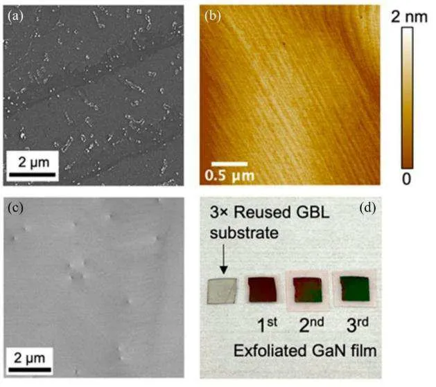
Fig. 3. GaN growth on the GBL. (a) The scanning electron microscopy(SEM)image of GaN grown on the GBL.(b)The atomic force micros copy(AFM)image of the surface of the GaN grown on the GBL.The root-meansquare(RMS)roughness is 0.18 nm. (c)Electron channeling contrast imaging(ECCI)image of GaN grown on the GBL,showing a total threading dislocation density of 2.1×107 cm-2. (d)Photograph of the three-times-reused GBL substrate and the exfoliated GaN epilayers.
Our group has also provided different insights into the interfacial interactions in RE from other perspectives. Quetal.[87]suggested that there was long-range orbital hybridization between the electronic states of the substrate and adsorbed atoms in RE, and that the crystallographic properties of the substrate played an important role in the in-plane orientation relationship between the nucleation layer and the substrate across the SLG. The adsorption energies of SLG on different substrates at different positions were calculated, demonstrating that polar substrates could greatly increase the adsorption ability of graphene to atoms,and the more polar the substrate (AlN>Al2O3), the greater its adsorption energy with adsorbed atoms (Fig. 4(a)). The differential charge density plot more visually shows that more charge transfer occurred in the Ga/SLG/AlN system, and the spacing between the Ga atoms and the SLG and AlN substrates was shorter compared to both of the other two systems (Figs. 4(b)–4(d)). Finally, a more intuitive analysis of the orbital hybridization between the bonded atoms was performed by calculating the partial density of states(PDOS)for the three systems mentioned above,as shown in Figs.4(e)–4(g). In the PDOS images,Ga-4p and Al-3p in the Ga/SLG/AlN system undergone orbital overlap near the Fermi energy level,even though the Ga and AlN substrates were far apart (~4.35 ?A), and this long-range orbital hybridization indicated the presence of strong chemical interactions between them.
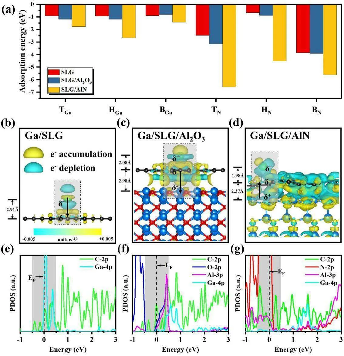
Fig.4. The influence of SLG with or without supporting substrate on the adsorption characteristics and electronic structure of Ga and N atoms on the surface of SLG.(a)Adsorption energy of Ga and N atoms at T,H,and B sites on SLG,SLG/Al2O3,and SLG/AlN substrates. CDD of(b)Ga/SLG,(c)Ga/SLG/Al2O3,and(d)Ga/SLG/AlN at H site. PDOS of(e)Ga/SLG,(f)Ga/SLG/Al2O3,and(g)Ga/SLG/AlN at H site.
3.3. Other epitaxy technologies
ELOG,namely selective area growth(SAG),was also an effective way to grow high-quality III-nitrides. Therefore,using graphene as a mask for ELOG could overcome the limitation that a large number of grain boundary defects were generated in QvdWE.
In 2013, Hanet al.proposed the first use of patterned graphene as a buffer layer for the ELOG of high-quality GaNbased devices. Scalable graphene oxide microscale patterns were generated using a combination of simple lithography and coating methods,which provided excellent heat dissipation for subsequent GaN-based LED devices while maintaining electrical and optical properties superior to those of LEDs grown on sapphire. From then on,ELOG of GaN using 2D materials as masks have been carried out by many research groups.[88]
In 2017, our group applied self-organized graphene as a nanomask in two-step epitaxial lateral overgrowth(2S-ELOG)of GaN.[89]A GaN film of about 20-μm thickness was formed on the GaN template by hydride vapor phase epitaxy(HVPE),showing low threading dislocation densities (TDDs) (3.6×108cm-2)and low strain(0.12 GPa)characterized using high resolution x-ray diffraction and Raman spectra,respectively.
In 2019, we also used the self-assembly nanoselective area growth (SNSAG) technology to obtain crack-free 150-μm thick GaN films on multilayer graphene(MLG)/SiC substrates with nanometer-sized mask (as shown in Fig. 5).[90]The TDDs of the film was about 5.9×106cm-2, showing a significant reduction compared to conventional epitaxial GaN films. The GaN films were nearly strain-free and could be mechanically exfoliated to obtain crack-free wafer-scale freestanding single-crystalline GaN. This suggested that SNSAG was a remarkably promising technology for wafer-scale integration of high-quality GaN with graphene for future applications in GaN-based devices.
Conventional ELOG techniques, such as using SiO2,SiNxas mask materials,[91–93]reduce dislocation density by blocking the extension of dislocations in the mask region,but also bring new problems,[94,95]including (i) strain cannot be relieved completely by ELOG,and the mismatch between the mask materials and films can also increase strain; (ii) thick mask materials can lead to small tilt angles in the epilayer when the adjacent epilayers at window regions mergence.
Graphene is used as the mask,which is an ultrathin mask with atomic-level thickness. In this ELOG/SAG technique,it is then able to reduce the stress and dislocation density in the epitaxial layer more effectively by reducing the mismatch with the epitaxial layer compared to a conditional dielectric mask.
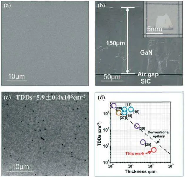
Fig.5. (a)Surface morphology of the GaN thick films formed by SNSAG on multilayer graphene (MLG)/SiC. (b) Cross-section SEM image of the GaN thick films formed by self-assembly nanoselective area growth(SNSAG)on MLG/SiC; the inset shows an image of crack-free free-standing GaN after release. (c) CL image of the GaN thick films. (d) The TDDs of GaN films formed by QvdWE (blue circle)/selective area growth (SAG) (purple circle)/RE (orange circle)/SNSAG (red circle) on graphene when compared with those formed by CE. The dashed line represents the influence of the thickness of the conventional epitaxial GaN films on TDDs.
3.4. The origin and evolution mechanisms of defects
At present, the main source of III-nitrides is heteroepitaxially grown on foreign substrates. However, due to the large lattice mismatch and difference in thermal expansion coefficient between the substrate and epilayer,the strain and dislocations generated in epilayer during the growth process. For example, the lattice mismatch between the sapphire substrate and GaN is as high as 16%,and the thermal expansion coefficient mismatch is 34%,so that the TDDs of GaN grown on it is as high as 108cm-2–1010cm-2.[96]The dislocation density greatly limits the application of III-nitrides devices.Therefore,studying the origin and evolution of defects on 2D materials is very important for the epitaxial growth of III-nitrides films.
Balushiet al.[82]studied the effect of graphene properties on GaN and AlN nucleation and they found that defective graphene was more conducive to nucleation. Therefore,the 2D materials have to be pretreated to change the surface chemical activity. Common methods include: bombarding the surface with plasma,[96]etching by passing NH3and other gases before growth,[70]obtaining poor quality 2D films by CVD,[97]etc.All in all, defects are introduced in different ways to provide nucleation sites for Ga, Al atom, and others,which resulted in more defects existing in III-nitrides.
We investigated the microstructural properties of defect at the interface of the GaN films grown using MOCVD on graphene/SiC substrates.[98]It was found that small-angle grain boundaries were ubiquitous in the GaN films grown on graphene,which was mainly present at the interface(as shown in Fig. 6). With the increase of the epitaxial thickness, the grain boundaries merged and thus decreased. The existence of grain boundaries was a typical feature of the QvdWE,[99]even if large scale single-crystal 2D materials were used as substrates. Therefore, this may be related to the interface force was weak vdW force.

Fig.6. (a)Cross-sectional TEM image of GaN films grown on graphene near the interface. (b) The SAED patterns were obtained from five different regions of GaN interface by TEM.And the corresponding torsion angle was given.
There are still a lot of stacking faults at the interface,which was caused by the lattice mismatch between graphene and GaN in theC-axis direction caused by the steps of the SiC substrates. This suggested thatC-axis lattice mismatch was still the origin of stacking faults in QvdWE. The main type of dislocation presented in GaN films was mixed dislocation,which was resulted in the coalescent of adjacent different GaN nucleation domains with different orientations.
The fabrication method of graphene has great influence on the crystal quality of III-nitrides. For transferred CVD graphene,high-angle grain boundaries could be found in GaN films with the TDDs of~1.3×109cm-2,[100]while for the transferred mechanicalexfoliation graphene, low-angle grain boundaries could be found in GaN films with the TDDs of 1.2×109cm-2–2.4×109cm-2.[101]It indicates that the polycrystalline of graphene make an important role on the crystal quality of III-nitrides. In 2019, Zhang’s group has improved the GaN crystalline quality greatly to the TDDs of 1.8×108cm-2by using a sputtered AlN/sapphire substrate.[102]The transfer process may introduce pollution onto 2D materials. Therefore,transfer-free 2D materials were more suitable for III-nitrides epitaxy. GaN (AlN) films grown on transferfree CVD graphene showed the TDDs of 1.7×10⁷(9.9×10⁸)cm-2.[103,104]In addition,for the epitaxial graphene from sublimation of SiC,the TDDs of GaN(AlN)films can realized to 2.1×10⁷(6.7×10⁸) cm-2,[105,106]which suggested that transfer-free 2D materials can be used to obtain higher quality III-nitrides.
In addition to the III-nitrides films epitaxy directly on 2D materials, 2D materials also played a crucial role in the process of ELOG. Zhanget al.[108]reported that the TDDs of 1.80×107cm-2and 1.09×107cm-2GaN films were ELOG on graphene and h-BN nanosheets using the HVPE method.They found that the dislocations in the substrate terminated under the 2D materials, resulting in a significant reduction in TDDs of GaN films. This report revealed that the mechanism of dislocation evolution using graphene and h-BN nanosheets as masks was similar to that of one-step epitaxial lateral overgrowth(1S-ELOG).
Subsequently,we used self-organized graphene as a nanomask for 2S-ELOG,[89]found that the evolution mechanism of dislocation was different from the conventional ELOG technique and the 1S-ELOG technique. A large number of dislocations could be seen at the initial interface of the GaN films fabricated by HVPE(HVPE-GaN)and MOCVD(MO-GaN),as shown in Fig. 7. Lattice mismatch may be created at the interface due to the growth of GaN buffer layer at low temperature,resulting in various orientations and a lot of dislocations formed at the interface.[70]For 2S-ELOG with graphene as a mask, besides the TDDs reduction, the differences were as follows: (i) Dislocations were annihilated at the interface of HVPE-GaN and MO-GaN.(ii)New dislocations were mainly produced at the summit of the triangle defective domains,which were the coalescence of different orientation domains and lateral-overgrown GaN.

Table 1. The TDDs of GaN or AlN films grown on graphene prepared by different methods.

Fig.7. The representative two-beam bright field TEM images of the HVPEGaN grown on MO-GaN without a graphene mask (a) g = 0002 and (b)g=11–20;with a graphene mask(c)g=0002 and(d)g=11–20.
3.5. Mechanical exfoliation and strain of nitrides on 2D materials
Due to the vdW force between 2D material and epilayer,lattice matches between epitaxial and substrate materials were not very strict,resulting in ultra-low residual strain of epitaxial III-nitrides. Therefore,nearly strain-free III-nitrides could be obtained and the epilayer could be mechanical stripping and transferred to foreign substrates.
In 2010, Chunget al.[70]achieved the transfer of GaN grown on graphene to foreign substrate for the first time. They grew high-density ZnO nanowalls on plasma-treated graphene as a buffer layer, and the grown GaN could be successfully transferred to foreign substrates. Kobayashiet al.[109]studied the GaN and GaN based LEDs QvdWE on h-BN, and found that GaN before and after the release was compressively strained and unstrained,respectively.
Our group has also studied on the growth of low-strain,exfoliable III-nitride materials on 2D materials. In 2020,Zhouet al.[75]reported strain-free GaN films QvdWE on PECVD graphene with a AlN buffer, which could be easily mechanical stripped. The E2(high)peak positions of the GaN films before(568.10 cm-1)and after(567.94 cm-1)released as shown in Fig. 8. Compared with the E2(high) peak position of strain-free GaN, the strain of this GaN film is only 0.023 GPa.
Also in 2020,Zenget al.[110]reported Raman analysis of E2(high)and A1-LO phonon to the strain-free GaN grown on sputtered-AlN/graphene buffer layer by comparing four GaN samples grown on different types of buffer layers (sputtered-AlN/graphene, MOCVD-AlN/graphene, graphene/MOCVDAlN and MOCVD-AlN) with MOCVD. Compared with the graphene on MOCVD-AlN, the intensity of D+D′scattering peak of graphene was more obvious on the sputtered AlN layer, which indicated the high density of defects provided higher nucleation for GaN.As shown in Fig.9,the frequency of E2(high) phonon of GaN epilayer on graphene/sputtered AlN was 568.2 cm-1, the closest to the strain-free GaN films.[111]On the other hand,the full width at half maximum(FWHM) of the E2(high) phonon scattering peak was distinctly the narrowest and the intensity was the largest on the graphene/sputtered AlN.
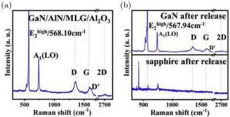
Fig.8. Raman spectra of(a)GaN/AlN/MLG/sapphire and(b)GaN film after released.
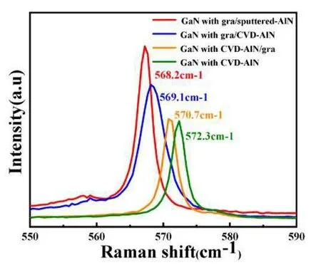
Fig.9. E2 (high)phonon of Raman spectra of GaN films grown on sapphire substrate with graphene/sputtered AlN buffer layer,graphene/MOCVD AlN buffer layer, MOCVD AlN/graphene buffer layer, and MOCVD AlN buffer layer in the low-wave region of 550 cm-1–590 cm-1.
4. Nitride device applications on 2D materials
For GaN materials with a wide direct bandgap(≈3.4 eV)and an exciton binding energy(≈24 meV),more and more attention has been paid to optoelectronic devices,such as LED,LD, and ohters. In 2012, Kobayashiet al., NTT Laboratory in Japan, successfully realized the epitaxial growth and stripping of GaN-LED on h-BN.[109]The 3-nm h-BN was grown on sapphire substrate by MOCVD, and then epitaxial highquality GaN films were grown on h-BN with an AlN buffer layer. The dislocation density was 8.6×109cm-2. After that,InGaN-LED was epitaxial on GaN films, and the separation of LED and substrate was successfully achieved by thermos releasing adhesive.
For comparison, the intensities of the electroluminescence increased with current (as shown in Fig. 10) and the electroluminescence intensities from the transferred LED were comparable to or higher than the intensities from the conventional LED on the low-temperature AlN buffer layer at the same current. This LED emitted blue light at room temperature.

Fig. 10. Electroluminescence of transferred and conventional LED at room temperature. (a)Current–voltage characteristics of the transferred LED.(b)Electroluminescence spectra from the transferred LED with currents ranging from 10 mA to 50 mA. (c) Electroluminescence spectra from the conventional LED with currents ranging from 10 mA to 50 mA.(d)Optical image of the bluelight electroluminescence from the transferred vertical-type LED.
In 2020,our group obtained epitaxial graphene with characteristic orientation on sapphire by PECVD, and then prepared metastable continuous flat GaN films with ultra-low biaxial compressive strain (0.023 GPa) by sputtering AlN buffer layer-assisted MOCVD.[75]The transferred GaN heterojunction was directly fabricated into a metal–insulator–semiconductor (MIS) devices from which typical electrical properties can be obtained.Heet al.fabricated hexagonal GaN microdisks using the multilayer graphene by HVPE.[112]The presence of a 2D buffer layer of graphene allowed GaN microdisks to be transferred to any substrate as desired. Then,under room temperature pulsed excitation,a double-triangular whispering-gallery mode (D3-WGM) multimode lasing was confirmed with a highQfactor of 3049 and an excitation threshold of about 11.5 μW in a single GaN microdisk.These results demonstrated the superior characteristics of D3-WGM lasing,which had potential applications in the fields of nanophotonics,lighting and optical communication.
In addition,GaN HEMT made with h-BN as a buffer layer can be transferred to other substrates with a simple mechanical exfoliation, and the substrates are recyclable. H-BN has the characteristics of high thermal conductivity and small dielectric constant. The HEMT device, made by Hirokiet al.from NTT laboratory,using h-BN as a buffer layer was transferred to the Cu substrate, which greatly inhibited the selfheating effect of the device and improved the performance of the device.[113,114]At the same time, due to its easy transferability characteristics,Glavinet al.used it to transfer to a flexible substrate to make a flexible radio-frequency device.[115]
The development of nitride fabrication technology on 2D materials is helpful to reduce the cost of nitride devices and realize high-quality III-nitride devices in order to extend its application. We believe that with the gradual realization of fine regulation of nucleation sites and in-depth understanding of the QvdWE or RE process of III-nitrides,the quality of IIInitrides on 2D materials will be further improved, and corresponding III-nitrides devices will be greatly developed.
5. Conclusion and perspectives
III-nitride epitaxy on 2D materials can effectively address the mismatch problems (lattice mismatch and thermal mismatch)caused by heterogeneous epitaxy and the development of substrate exfoliation techniques to obtain high-quality,lowcost III-nitride materials for high-quality III-nitride devices and their extension in the field of flexible wearable electronics.
This paper describes the preparation of some common 2D materials(e.g.graphene,h-BN),mainly summarises the common methods for epitaxial III-nitride on 2D materials and addresses the defects and stresses in III-nitride,and finally mentions some applications of III-nitride on 2D materials for devices. Specifically, the common techniques for epitaxial IIInitride on 2D materials with their characteristics are as follows.
(i) QvdWE. The interfacial mismatch problem of IIInitride materials was significantly improved by QvdWE due to its weak van der Waals forces at the interface, and the advantages of low strain and peelability were given. At the same time,the growth rate of the III-nitride material was significantly increased due to the growth mode. However, the weak van der Waals forces were a double-edged sword,which leaded to an increase in the number of tilted grains in the III-nitride material during growth, which in turn leads to an increase in the dislocation density with a spiral component,making the predominant dislocation type in QvdWE predominantly mixed dislocations. In addition, the low surface energy of 2D materials makes III-nitride nucleation difficult in the early stages of growth. The solution was to create defects and insert buffer layers(e.g.ZnO,AlN)predominantly on 2D materials.
(ii) RE. RE has been proposed with the idea that the charge of the polar substrate could “penetrate” the graphene and act on the epitaxial layer, thus facilitating the fabrication of single-crystal III-nitride materials without grain boundary defects. Our team believed that there was a remote orbital hybridisation effect between the substrate and the adsorbed atoms in remote epitaxy. At present,the relationship between growth mechanisms and interfacial interactions in RE was less studied,and its profound physical nature was yet to be further investigated.Research into the scientific aspects of remote epitaxy was expected to break through the inherent properties of large mismatch heterogeneous epitaxy of III-nitrides and drive a completely new transformation of III-nitride epitaxy technology.
Furthermore, the strategy of polarization-driven orientation-selective growth was proposed in 2022,[116]based on the principle of tuning the energy profile of the system by means of an applied electric field. In other words,i.e.polarization can change the orbital energy level to produce the most favorable orbital coupling. This provides the idea that an electric field can be appliedin situto control the epilayer polarity and orientation during the growth of nitrides on 2D materials,hopefully making it possible to realize single-crystal nitrides on arbitrary substrates.
Acknowledgments
Project supported by the State Key Program of the National Natural Science Foundation of China (Grant No. 61734008) and the National Natural Science Foundation of China(Grant No.62174173). Thanks to Yipu Qu, Yuning Wang, Lu Li, Fan Yang, Jianjie Li, Jiahao Tao, Xin Cai, Jinbiao Huang,Jizong Zhou,Yunpeng Wu,and Meng Le for their preparing the manuscript.

- Chinese Physics B的其它文章
- Microwave absorption properties regulation and bandwidth formula of oriented Y2Fe17N3-δ@SiO2/PU composite synthesized by reduction–diffusion method
- Amplitude modulation excitation for cancellous bone evaluation using a portable ultrasonic backscatter instrumentation
- Laser-modified luminescence for optical data storage
- Electron delocalization enhances the thermoelectric performance of misfit layer compound(Sn1-xBixS)1.2(TiS2)2
- TiO2/SnO2 electron transport double layers with ultrathin SnO2 for efficient planar perovskite solar cells
- Sputtered SnO2 as an interlayer for efficient semitransparent perovskite solar cells