
Defect physics of the quasi-two-dimensional photovoltaic semiconductor GeSe
2022-11-21 09:40:08SaichaoYan閆賽超JinchenWei魏金宸ShanshanWang王珊珊MenglinHuang黃夢(mèng)麟YuNingWu吳宇寧andShiyouChen陳時(shí)友
Chinese Physics B 2022年11期
關(guān)鍵詞:王珊
Saichao Yan(閆賽超) Jinchen Wei(魏金宸) Shanshan Wang(王珊珊) Menglin Huang(黃夢(mèng)麟)Yu-Ning Wu(吳宇寧) and Shiyou Chen(陳時(shí)友)
1Key Laboratory of Polar Materials and Devices(MOE)and Department of Electronics,East China Normal University,Shanghai 200241,China
2State Key Laboratory of ASIC and System,School of Microelectronics,Fudan University,Shanghai 200433,China
GeSe has recently emerged as a photovoltaic absorber material due to its attractive optical and electrical properties as well as earth abundancy and low toxicity. However, the efficiency of GeSe thin-film solar cells (TFSCs) is still low compared to the Shockley–Queisser limit. Point defects are believed to play important roles in the electrical and optical properties of GeSe thin films. Here, we perform first-principles calculations to study the defect characteristics of GeSe.Our results demonstrate that no matter under the Ge-rich or Se-rich condition, the Fermi level is always located near the valence band edge,leading to the p-type conductivity of undoped samples. Under Se-rich condition,the Ge vacancy(VGe)has the lowest formation energy, with a (0/2–) charge-state transition level at 0.22 eV above the valence band edge. The high density(above 1017 cm-3)and shallow level of VGe imply that it is the p-type origin of GeSe. Under Se-rich growth condition, Sei has a low formation energy in the neutral state, but it does not introduce any defect level in the band gap,suggesting that it neither contributes to electrical conductivity nor induces non-radiative recombination. In addition, Gei introduces a deep charge-state transition level, making it a possible recombination center. Therefore, we propose that the Se-rich condition should be adopted to fabricate high-efficiency GeSe solar cells.
Keywords: GeSe bulk,point defect,concentration,photovoltaic
1. Introduction
As potential alternatives to silicon-based photovoltaic systems,thin-film solar cells(TFSCs)have attracted considerable attention due to the advantages of low-cost constituents,high stability, high efficiency and device flexibility.[1–7]Statistically, the power conversion efficiencies (PCEs) of copper indium gallium selenide (CIGS) and cadmium telluride(CdTe)have reached 23.4%and 22.1%,respectively.[8,9]Nevertheless, In and Te are relatively rare elements, and Cd is toxic. These shortcomings limit the development of these TFSCs. Therefore, there is a great need to discover a new material with non-toxic and earth-abundant elements. In the past decade, many absorber materials have been investigated, such as CZTSSe,[10]SnS,[11–15]Sb2(S,Se)3,[16–22]Cu2O,[23–25]CuSbSe2[26,27]and GeSe.[28–36]Among these materials, GeSe has received increasing attention in recent years.
GeSe can be used as a new and durable photovoltaic absorber for the following reasons: (1) The element Ge and Se are abundant on earth and low-toxic in nature, making it preferable compared to classic CdTe and CIGS.[28](2) GeSe has a low melting point of 670 °C, which makes it ideal for producing high-quality films at low temperatures.[29](3)GeSe has sublimation properties, allowing simultaneous thin film deposition andin-situraw material purification, and can also be limited by impurities in the sublimation source. The sublimation feature can also prevent the formation of unfavorable Ge and Se interstitials.[30,31](4) GeSe has an acceptable band gap of 1.1–1.2 eV, which is within the optimal bandgap value for a single junction solar cell, according to both experimental and theoretical analysis.[32,33]In the visible light range, it also possesses a high optical absorption coefficient of over 104cm-1, allowing full light absorption within a one-millimeter-thick layer.[34](5) GeSe crystallizes in layered structures with few and weak dangling bonds between the layers,resulting in great chemical stability and low surface defect density,as demonstrated by theoretical and experimental researches.[35](6)GeSe has the cation–anion antibonding states-derived valence band maximum, like the case of CuSbSe2.[26]
Despite the aforementioned advantages and significant attempts to optimize GeSe solar cells,[36–42]their performance remains subpar compared to the Shockley–Queisser efficiency limit of up to 30%. Hence, it is in great need to propose new optimizing approaches and break through the bottleneck.Among different aspects that can affect the photovoltaic performance of GeSe, the defect properties should be one of the priorities. Although the lone pair existing in the VBM has been regarded as the advantage of GeSe to be defecttolerant,[36]the influence of defects on the electrical properties of GeSe is not well explored. What are the possible recombination centers in GeSe? How are the conductivity and defect density changed using different growth conditions? To gain a comprehensive understanding of the defect physics in GeSe,we calculate the defect properties of GeSe and the pinning Fermi level under different growth environments via the firstprinciples calculations.The results show that VGehas the lowest formation energy under Se-rich condition, with a (0/2-)charge-state transition level lying 0.22 eV above the VBM.The shallow level and high density (over 1017cm-3) of VGesuggest that it is the p-type origin of GeSe. Seiin neutral state also has low formation energy under Se-rich growth condition,consistent with the layered structure of GeSe that can easily hold interstitial Se atoms. Only neutral state can be found for Sei, indicating that it neither contributes to the conductivity,nor causes the recombination. Besides, it is also noted that changing the growth condition from Se-rich to Se-poor will not affect the p-type conductivity because of the Fermi level pinning close to the VBM, but the Se-poor condition favors the formation of Gei, which is a possible recombination center due to its deep charge-state transition levels. Therefore,we propose that better GeSe photovoltaic thin film should be grown under the Se-rich condition.
2. Methods
The Viennaab initiosimulation software (VASP) with a plane wave basis set was used for all first-principles calculation.[43,44]Frozen-core projector augmented-wave(PAW) pseudopotentials with an energy cutoff of 350 eV were employed, with a 10×8×4Γcenteredk-point mesh included in the Brillouin zone integration for the primitive cell. In the calculations of defect properties, we built a 128-atom supercell with a singleΓpoint to reduce the correlation between defects.[45]For the crystal structure optimization, the exchange–correlation functional that we used was the generalized gradient approximation (GGA)of Perdew–Burke–Ernzerhof (PBE).[46]Meanwhile, the hybrid exchange–correlation functional (HSE) with a fractionα=17% of Hartree–Fock exchange was used for the static calculation of the total energy.[47,48]Since GGA usually underestimates the band gap for these compounds,the HSE functional predicted the band gaps with better agreement with experimental results for GeSe. Both methods included the D3 dispersion correction of Grimmeet al.[49]It has been demonstrated that including such a dispersion correction improves the structural description of layered and low-dimensional posttransition metal chalcogenides: PBE+D3 has recently been utilized to compute the Sn(S,Se) solid solution,[50]while HSE+D3 has been demonstrated to mimic the experimental structure and electrical characteristics of the pseudo-1D chalcogenide Sb2Se3.[51–53]
The defect calculation is performed by using defect and dopantab-initiosimulation package (DASP).[54]The neutral formation energies can be calculated with the expression

Here,E(α)is the calculated total energy of the supercell with a defectα,E(host)is the total energy of the pure GeSe supercell,niis the number of atoms of elementiadded into (niis negative) or removed from (niis positive) the supercell,μiis the elemental chemical potential andE(i)is the total energy of pure elemental phase.μi=0 means that the element is so rich that even its pure elemental phases can form. We also calculate the formation energy of GeSe in the ionized charge stateq,and the formula of formation energies is[55]
whereEFis the Fermi energy referenced to the VBM level,andEVBMis the energy of the VBM level of host.
The equilibrium densityn(α,q) of a defect in its charge stateqis a function of its formation energy,which can be given by[56]
where ΔEf(α,q) is the defect formation energy,Nsitesis the number of defect sites per unit volume,gqis the degeneracy factor, which reflects the number of possible configurations for electrons occupying the defect level and changing with the charge stateq,KBis the Boltzmann constant,andTis the temperature. Because ionized defects create carriers and become charged,we can calculate the charge density of all ionized acceptor defects (N-A) and all ionized donor defects (N+D). The density of carriers follows

whereNvandNcare the effective densities of states for the valence band and conduction band edges, respectively. The Fermi level (EF), carrier density and density of all point defects in different charge states under different chemical potential conditions can be determined by solving self-consistently the charge-neutrality condition[57–59]
It is assumed that defects are generated at high temperatures, and the densities in different charge states are redistributed when the temperature cools down to working temperatures. Accordingly, we first solve Eq.(5)at a higher growth temperature and then determine the Fermi level and density of each defect for different charge statesq. Then Eq. (5) is solved again at a lower working temperature, but the defect density in different charge states will redistribute according to the Fermi–Dirac occupation. The Fermi level at the working temperature can then be obtained,from which the redistributed defect density and carrier density can be calculated.
3. Results and Discussion
3.1. The progress of GeSe thin-film solar cells
We first review the experimental progress of GeSe TFSCs and the corresponding performance parameters of GeSe TFSCs are summarized in Table 1. The first GeSe solar cell was reported by Wan’s group in 2017.[31]They used self-regulated fast thermal sublimation to create high-quality GeSe thin films on a CdS buffer layer, and built a superstrate ITO/CdS/GeSe/Au solar cell with a power conversion efficiency (PCE) of 1.48%, fill factor (FF) of 42.6%, shortcircuit current density (JSC) of 14.48 mA/cm2and an opencircuit voltage (VOC) of 240 mV.[31]In 2018, Huanget al.reported the GeSe films fabricated by magnetron sputtering and constructed a prototypical FTO/CdS/GeSe/carbon/Ag device with a PCE of 0.05%,FF of 26.5%,JSCof 0.85 mA/cm2andVOCof 220 mV.[60]Moreover, Chenet al. preparedα-GeSe precursor thin films using thermal evaporation and p-GeSe thin films using a sandwiching post-annealing process. They also prepared a superstrate cell with FTO/TiO2/p-GeSe/carbon/Ag configuration demonstrated an amazingVOCof 340 mV, efficiency of 0.27%, FF of 25.15% andJSCof 3.19 mA/cm2.[61]In addition, Ziet al. applied thermal evaporation to create GeSe films and FTO/CdS/GeSe/Au devices with a PCE of 0.65%, FF of 38.2%,VOCof 135 mV,andJSCof 12.6 mA/cm2.[62]Despite significant attempts to produce GeSe solar cells, their performance remains subpar, with a Shockley–Queisser efficiency limit of up to 30%. Recently,Liuet al. demonstrated that surface defects in GeSe photovoltaics had a significant impact on the device performance and created surface-passivated GeSe solar cell.[36]The PCE of the surface-passivated GeSe solar cells is 5.2% and is higher 3.7 times than the best previously-reported GeSe results.For other performance,the FF is 56%,theVOCcan reach 380 mV, and theJSCis 24.6 mA/cm2. Hu’s group proposed that this can be caused by the superstrate device structure,and they fabricated two GeSe solar cells with superstrate and substrate configurations.[63]For the superstrate configurations(glass/ITO/CdS/GeSe/Au),the PCE is 1.4%,the FF is 39.2%,theVOCis 230 mV and theJSCis 15 mA/cm2. Compared with the superstrate configurations,the pristine substrate configuration(glass/Mo/GeSe/CdS/iZO/ITO/Ag)exhibits PCE of 2.7%,FF of 41.3%,VOCof 330 mV andJSCof 19.8 mA/cm2.To improve the PCE of GeSe solar cells with substrate configurations,they optimized the annealing temperature of complete devices via a self-developed high-throughput method. By annealing the pristine substrate solar cell at 150 °C, they found the PCE of the substrate solar cell is 3.1%, FF is 47.1%,VOCis 330 mV andJSCis 20.1 mA/cm2. The PCE is twice that of the best previously reported superstrate GeSe solar cell.
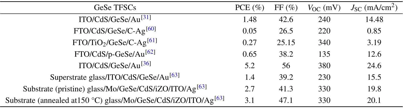
Table 1. The performance of GeSe thin-film solar cells.
Given the high theoretical efficiency limit of~30% for GeSe solar cells,there is still a lot of potential to enhance the efficiency of GeSe thin-film solar cells compared to other popular thin-film photovoltaics like CdTe and CIGS. In terms of experiments, Liuet al. proposed multiple strategies to improve the efficiency of GeSe TFSCs:[31](1) exploring preparation methods that can improve the quality of GeSe thin films, (2) controlling the orientation of GeSe film, (3) finding a more suitable buffer layer, (4) using hole transport materials (HTM), and (5) constructing a solar cell with a substrate structure. Besides,Yanget al.also proposed some improvement strategies:[64](1)developing more facile and effective deposition techniques,(2)developing solution processing method suitable for simple binary GeSe thin film preparation,(3) exploring proper partner materials, such as n-type buffer and hole transport layer by computational. In terms of theoretical research,Lvet al.[38]found that the PCE for AB-stacked GeSe/SnS heterostructures TFSC can be as high as~18%by using first-principles calculations. Meanwhile, Maoet al.[39]predicted that the PCE of the GeSe/SnSe heterostructure TFSC can reach 21.47% based on first-principles calculations. Although there are many theoretical studies on the photoelectric properties of GeSe, there are few reports on the effect of defect characteristics on the photoelectric properties of GeSe. In fact,the defects properties are critical to the photovoltaic performance of GeSe. For example, shallow-level defects can control semiconductor conductivity, while deep-level defects can promote the recombination of the non-equilibrium carriers in an excited state, thereby reducing the efficiency of the solar cells. Therefore, we will study the defect properties of GeSe in the next part.
3.2. The properties of GeSe defect
The GeSe has a layer-type orthorhombic structure with space groupPnma, as shown in Fig. 1. The unit cell contains eight atoms,and each Ge or Se is three-fold coordinated.Table 2 presents the optimized lattice constants, along with the experimental and other theoretical results for comparison.The relaxed lattice parametersa=3.88 ?A,b=4.50 ?A, andc=10.99 ?A,which are slightly larger than those experimental values ofa=3.81–3.85 ?A,b=4.37–4.41 ?A,andc=10.78–10.84 ?A[30,64–66]due to the overestimation lattice constants using the GGA method. For other calculations,the calculated lattice constants range from 3.83 ?A to 3.91 ?A,4.33 ?A to 4.49 ?A,and 10.85 ?A to 11.31 ?A fora,b,andc,[67–70]respectively. Our results are in reasonable agreement with others’results.
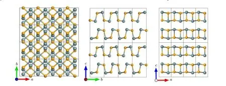
Fig.1. Crystal structure of GeSe bulk from different view angles. Ge atoms are represented in gray,Se atoms are represented in orange,and each small rectangle represents a primitive cell.
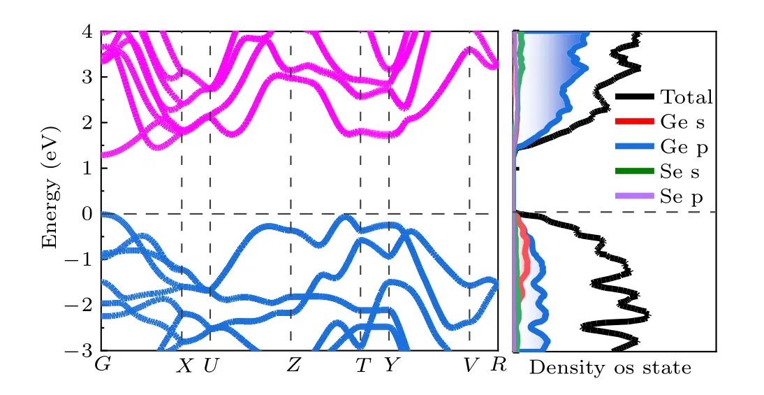
Fig.2. Calculated band structure,density of states(DOS),and partial DOS projected on different elements of GeSe.

Table 2. The calculated lattice constants of GeSe. The experimental and theoretical results in the literatures are listed for comparison.
Due to the fact that the electronic properties of point defects depend sensitively on the electronic structure, we calculate the band structure, density of states (DOS), and partial DOS of GeSe, as shown in Fig. 2. The direct band gap is 1.33 eV, and the conduction band minimum (CBM) and valence band maximum (VBM) are located at theΓhighsymmetry point. From the DOS, the CBM of GeSe is dominated by the Ge p orbital, with significant coupling with the Se p orbital and negligible coupling with the Se s orbital while the VBM of GeSe is mainly contributed by the Ge s and p orbitals.
Because most of previous calculations only considered defects with neutral charge state,for comparison,we first calculate the formation energies of neutral defects in GeSe.There are six common types of intrinsic point defects in GeSe:cation vacancy (VGe), anion vacancy (VSe), cation interstitial (Gei),anion interstitial (Sei), cation-on-anion antisite (GeSe), and anion-on-cation antisite (SeGe). Table 3 presents the neutral formation energies of GeSe defects under both Se-rich and Gerich conditions calculated by us and others. For GeSe under Ge-rich condition,the formation energies are 1.37 eV,1.71 eV,1.92 eV, 1.26 eV, 1.45 eV and 1.90 eV for VGe, VSe, Gei,Sei, GeSeand SeGe, respectively. These values are comparable to the results of Liuet al.[36]under Ge-rich condition,the formation energies of VGe, VSe, Gei, Sei, GeSeand SeGeare 1.34 eV, 1.59 eV, 2.19 eV, 2.32 eV, 1.54 eV and 2.29 eV,respectively. Under Se-rich condition,the formation energies are decided to be 0.83 eV,2.24 eV,2.46 eV,0.72 eV,2.52 eV and 0.83 eV for VGe, VSe, Gei, Sei, GeSeand SeGe, respectively,which are also consistent with the corresponding values of 1.25 eV, 1.66 eV, 2.28 eV, 2.24 eV, 1.71 eV and 2.12 eV reported by Liuet al. Our results indicate that both VGeand Seimay have important influences on the electrical and optical properties of GeSe, since their formation energies of neutral defects are lower than 1 eV under Se-rich condition,meaning that their concentrations are high. However, different results have been obtained by other groups,[36,71–73]who carried out GGA-PBE calculations on GeSe by using different supercells,and found Seihas a higher formation energy than our results under both Se-rich and Ge-rich conditions. For the Sei, we consider multiple interstitial sites by using DASP,from which we search for the low-energy configurations after performing calculations for all sites. The Seistructure with the lowest energy is shown in Fig. S1 of the supplementary material. It is noted that the formation energy of Seiis lower than that of other defects under both Ge-rich and Se-rich growth conditions, consistent with the layered structure of GeSe that can easily hold interstitial atoms.
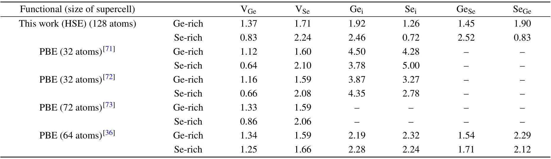
Table 3. The neutral formation energies(in eV)of the defects in GeSe under both Se-rich and Ge-rich conditions calculated in this work and by others.
To further explore the defect properties of ionization,we also calculate the formation energy and transition level of the above six defectsαin different ionized charge states. The formation energies of all defects (VGe, VSe, Gei, Sei, GeSe, and SeGe) in the most stable charge states are plotted as a function of the Fermi level, as shown in Fig.3. Obviously, under both Se-rich and Ge-rich conditions,Seiand SeGeare most stable in neutral state, and their formation energies are constant in the whole Fermi level range. Under the Ge-rich condition(Fig.3(a)),if the Fermi level sits at VBM,VGeis in the neutral state,and the formation energy of Ge2-i is lower than those of other defects. VGestays neutral until the Fermi level rises to 0.22 eV above VBM. VGebecomes-2 charged and its formation energy decreases as the Fermi level rises from 0.22 eV above VBM to CBM. It eventually becomes the defect with lowest formation energy. Geiis in +2 state and its formation energy keeps increasing between VBM and 0.54 eV below CBM. For the Fermi level between 0.54 eV below CBM and CBM, Geibecomes neutral and the formation energy keeps unchanged. This causes the Fermi level to be pinned near the VBM,indicating that GeSe is a p-type semiconductor. Under the Se-rich condition (Fig. 3(b)), a similar pattern can be observed as the Fermi level raises from VBM to CBM, except that the lowest formation energy of Geiis always higher than the highest formation energy of VGe. In addition,there are no intrinsic defects to compensate with VGe,so the Fermi level is also located near VBM.Therefore,the conductivity of GeSe is always p-type under different growth conditions, because the Fermi level is pinned near the VBM. The result is consistent with the experimental results that GeSe is an intrinsic p-type semiconductor.[30,31,74,75]

Fig.3.The formation energies of intrinsic defects in GeSe under(a)Ge-rich and(b)Se-rich conditions as functions of the Fermi energy.
The calculated transition levels of the intrinsic defects in the band gap of GeSe are summarized in Fig. 4. The transition level of SeGeis 0.04 eV below VBM,and Seialso has no transition level in the band gap. Hence,it is worth noting that although Seihas a lower formation energy, it does not affect the conductivity and cause the recombination due to the lack of charge state.VGehas a defect level of(0/2–),which is 0.22 eV from VBM,indicating that VGeis a shallow accepter and the p-type origin of GeSe. In contrast,(0/2+)defect level of Geiis deep in the bandgap,or 0.54 eV below CBM.For GeSeand VSe, they both have two transition levels. The (0/2+) level of GeSeis located at 0.07 eV above the VBM,and the(0/2–)level is located at 0.42 eV below the CBM,that is,the acceptor defect level is shallower than the donor defect level. On the contrary, for VSe, the donor defect level is shallower than the acceptor defect level. Specifically,the(0/2+)defect level of is 0.47 eV higher than VBM,and the(0/2–)defect level is 0.17 eV lower than CBM.
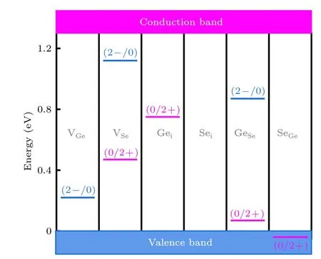
Fig. 4. The calculated charge-state transition levels of the intrinsic defects in the bandgap of GeSe. The blue bars show the acceptor levels, and the pink bars represent the donor levels. The initial and final charge states are labeled in parentheses.
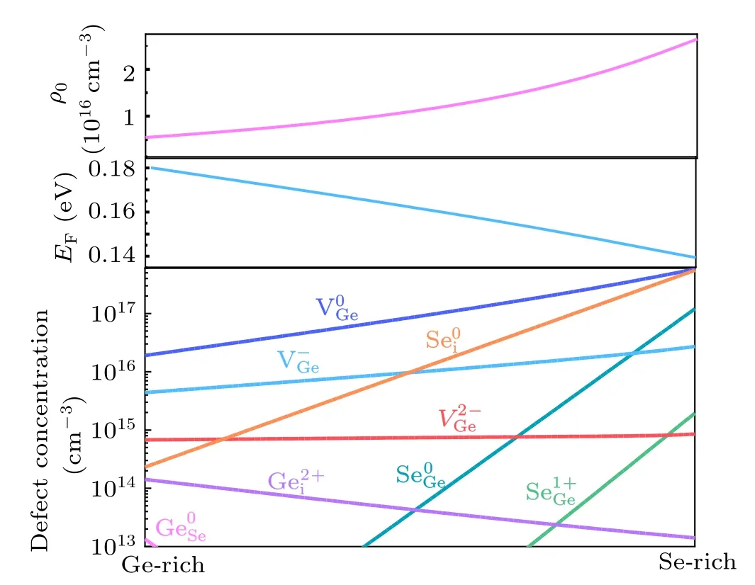
Fig. 5. Calculated density of all intrinsic points defects, Fermi levels, and hole-carrier density at room temperature(300 K)in GeSe crystals grown at a high temperature(800 K)under different chemical conditions.
The calculated density of all intrinsic point defects in different charge states, Fermi level, and hole-carrier density changing with the chemical condition are shown in Fig.5.The concentrations of VGe, Sei, and SeGeincrease as the growth condition changes from Ge-rich to Se-rich, whereas the concentrations of Geiand GeSedecrease. This is consistent with the calculated formation energies. The concentrations of VGeand Seiunder Se-rich condition are in the order of 1017cm-3and 1014cm-3under Ge-rich condition, respectively. However,Seistays at neutral state and does not affect conductivity or recombination, so VGeis the dominate defect. Therefore,the high concentration of VGeis the reason why GeSe is the p-type semiconductor. Furthermore, the concentration of Geiis higher than 1014cm-3under Ge-rich condition, indicating that Ge-rich condition favors the Geigeneration. Owing to its deeper charge-state transition level probably being the recombination centers, we propose growing GeSe thin film under Se-rich condition to prevent the formation of deep-level defect Gei.
4. Conclusion
In summary, we systematically investigate the point defects of GeSe using first-principles calculations under different growth conditions. The results show that VGehas the lowest formation energy under Se-rich condition, with a (0/2–)charge-state transition level lying 0.22 eV above the VBM.Hence,the p-type origin of GeSe mainly contributes from the shallow level and high density(over 1017cm-3)of VGe. Under Se-rich growth condition,Seihas a low formation energy in the neutral state,which is consistent with the layered structure of GeSe,which can easily hold interstitial atoms. Seihas no charge state, implying that it neither contributes to conductivity nor is responsible for recombination. Furthermore,because the Fermi level is pinned near VBM, adjusting the growth condition from Se-rich to Se-poor has little effect on the p-type conductivity. However, Ge-rich condition favors the formation of Gei,which is a probable recombination center because of its deep charge-state transition levels. Therefore, we recommend that better GeSe thin film can be grown under Se-rich condition.
Acknowledgments
This work was supported by Shanghai Academic/Technology Research Leader(Grant No.19XD1421300),the National Natural Science Foundation of China (Grant No. 12174060), Program for Professor of Special Appointment (Eastern Scholar TP2019019), the National Key Research and Development Program of China (Grant No. 2019YFE0118100), State Key Laboratory of ASIC &System (Grant No. 2021MS006) and Young Scientist Project of MOE Innovation Platform.
猜你喜歡
瘋狂英語(yǔ)·讀寫(xiě)版(2023年1期)2023-05-30 10:48:04
大眾文藝(2022年17期)2022-09-27 16:05:50
瘋狂英語(yǔ)·讀寫(xiě)版(2022年11期)2022-05-30 01:22:33
民族文匯(2022年17期)2022-05-16 21:01:51
健康體檢與管理(2022年2期)2022-04-15 01:33:37
瘋狂英語(yǔ)·讀寫(xiě)版(2021年10期)2021-12-14 13:13:10
瘋狂英語(yǔ)·新讀寫(xiě)(2021年10期)2021-12-07 02:41:30
金秋(2020年4期)2020-08-18 02:39:20
37°女人(2018年8期)2018-08-23 05:59:06
幸福家庭(2018年8期)2018-08-23 05:35:56

- Chinese Physics B的其它文章
- Microwave absorption properties regulation and bandwidth formula of oriented Y2Fe17N3-δ@SiO2/PU composite synthesized by reduction–diffusion method
- Amplitude modulation excitation for cancellous bone evaluation using a portable ultrasonic backscatter instrumentation
- Laser-modified luminescence for optical data storage
- Electron delocalization enhances the thermoelectric performance of misfit layer compound(Sn1-xBixS)1.2(TiS2)2
- TiO2/SnO2 electron transport double layers with ultrathin SnO2 for efficient planar perovskite solar cells
- Sputtered SnO2 as an interlayer for efficient semitransparent perovskite solar cells