
Uniform light emission from electrically driven plasmonic grating using multilayer tunneling barriers
2022-01-23 06:35:10XiaoBoHe何小波HuaTianHu胡華天JiBoTang唐繼博GuoZhenZhang張國(guó)楨XueChen陳雪JunJunShi石俊俊ZhenWeiOu歐振偉ZhiFengShi史志鋒ShunPingZhang張順平ChangLiu劉昌andHongXingXu徐紅星
Chinese Physics B 2022年1期
Xiao-Bo He(何小波) Hua-Tian Hu(胡華天) Ji-Bo Tang(唐繼博) Guo-Zhen Zhang(張國(guó)楨)Xue Chen(陳雪) Jun-Jun Shi(石俊俊) Zhen-Wei Ou(歐振偉) Zhi-Feng Shi(史志鋒)Shun-Ping Zhang(張順平) Chang Liu(劉昌) and Hong-Xing Xu(徐紅星)
1School of Physics and Technology,Center for Nanoscience and Nanotechnology,
and Key Laboratory of Artificial Micro-and Nano-structures of Ministry of Education,Wuhan University,Wuhan 430072,China
2Shandong Provincial Engineering and Technical Center of Light Manipulation and Shandong Provincial Key Laboratory of Optics and Photonic Devices,School of Physics and Electronics,Shandong Normal University,Jinan 250014,China
3The Institute for Advanced Studies,Wuhan University,Wuhan 430072,China
4Key Laboratory of Materials Physics of Ministry of Education,School of Physics and Microelectronics,
Zhengzhou University,Zhengzhou 450052,China
Keywords: electroluminescence, plasmonics, inelastic electron tunneling, multilayer insulator, atomic layer deposition
1. Introduction
Light emission by inelastic tunneling (LEIT) through a tunnel junction can offer unique opportunities to realize ultrafast electrical-optical-signal transduction,[1,2]which can generate light below the diffraction limit and provide potential applications in nanoscale biosensing,[3,4]optical communication,[5]and integrated photonics circuits.[6]First demonstrated by Lambe and McCarthy in 1976,[7]the tunneling electrons in a planar metal-insulator-metal(MIM)tunnel junction will excite the surface plasmons and may subsequently decay into far-field photons. This luminescence process is in principle ultrafast because the timescale for an electron tunneling through the junction proves to be on the order of 10 fs (the excitation process), and the lifetime of an emitter in the nanogap can be shortened to tens of fs(the emission process).[8,9]This phenomenon is then used to visualize the local density of states in scanning tunneling microscopes[10-13]until recently it has received considerable renewed interest in electrically-driven optical antennas.[14,15]Significant advances have been made since then,including the improvement of the emission efficiency,[16,17]radiation directionality,[18]and spectra shape[19-21]of the MIM tunnel sources. The stability of an LEIT device, a key operation figure of merit, depends significantly on the fabrication of the tunnel barrier.Till now, a highly stable tunnel barrier has relied mainly on the synthesis of a dense insulator layer between the biased metal structures,by,e.g.,thermal oxide,[22]exfoliated hexagonal boron nitride,[23]or self-assemble molecules.[24]However, these methods are either hard to control the thickness(oxidization) or incompatible with the modern microfabrication streamline,hindering the LEIT devices from being manufactured and put into practical applications.
Atomic layer deposition(ALD)is a well-developed technique of depositing thin films in microelectronics,[25,26]lightemitting diodes,[27]hot-electron electrochemistry,[28]and diffusion barrier coatings with low gas permeability.[29]The uniqueness of ALD in these applications is attributed to its ability to grow the uniform,pinhole-free,and nanometer-thick insulator layers.[30,31]However,the operation of LEIT devices with a single Al2O3layer grown by ALD is unstable under ambient condition due to the formation of grains and defects during the growing process.[32]Therefore, it is necessary to obtain high-quality tunnel insulators by ALD so that the fabrication of LEIT devices is fully compatible with microfabrication techniques.
2. Method
2.1. Device fabrication
Electrically driven plasmonic gratings are fabricated on Si/SiO2substrate. The thickness of the SiO2layer is 300 nm that can efficiently reduce the leak current. The bottom Au electrode is prepared by a series of fabrication steps,including EBL, reaction-ion etching (RIE, using CHF3gas flow), and thermal evaporation of Au film(50 nm). After lift-off,the O2plasma treatment process in an RIE is used to generate the high hydroxyl density substrate,in which the treatment power is 50 W and the treatment time is 1 min. The treated sample is then grown on the multiple insulator layers by ALD at a temperature of 150°C. Then, the top gratings are prepared by the EBL, Au evaporation, and lift-off. The details of the fabrication process are shown in the supporting information,Fig.S1.
2.2. Electrical and optical characterization
For electrical measurements, two tungsten probes with 10-μm diameter are used to contact the Au electrodes with a sourcemeter(Keithley 2634B).The parameters are 5 NPLC(number of power line cycles) for the analog-to-digital converter,integration times of 1 s,and the current using the automatic range switch. The EL images are recorded by an optical microscope (Olympus BX51) equipped with a 50× long working distance objective (NA = 0.5) and a CCD camera(DVC 710M-00-MW).The emission spectrum is collected by a spectrometer(Andor 550i,150 lines/mm blazing at 800 nm)and detected by the EMCCD (Andor Newton). The reflection spectrum is collected by a home-built microscope using a 100×objective(NA=0.9)and the diameter of the white light spot is 2μm.
2.3. Electromagnetic simulations
Full wave electromagnetic simulations are carried out by commercial FEM software (COMSOL Multiphysics, V5.2a).A two-dimensional model is established by considering the grating positioned on the top of an Au film. The permittivity of Au is cited from the Johnson and Christy.[40]The insulator gaps within the structures have a thickness of 4.0 nm and a refractive index of 2.05.
3. Experiment and results
In this work, we fabricate an LEIT device with uniform light emission and a long working lifetime under ambient condition, by optimizing the composition during the ALD growth. For the first time, we grow alternative insulator layers (TiO2-Al2O3-TiO2-Al2O3) as the tunnel barrier,in a fully microfabrication-compatible manner. Our devices can be stored for a long time (several weeks) and the tunneling current keeps stable for intermittent measurements from hours to days. The light emission is uniform in the entire active region, and the emission spectra can be controlled by a plasmonic grating. Our study demonstrates that the multilayer insulators grown by ALD enable a stable and uniform LEIT device. Furthermore, the composite tunnel barrier may also provide an additional degree of freedom for the band structure of the tunnel barrier[33,34]or find applications in other ultrafast electro-optical circuits. Figure 1(a) shows the schematic of an LEIT device. It consists of a square bottom Au electrode, alternate insulator (TiO2-Al2O3) layers, and a top Au plasmonic grating simultaneously serving as a coupler for light and a positive electrode. The bottom Au electrode and the top plasmonic grating are prepared by electron beam lithography(EBL),and both layers are 50-nm thick.The grating is aligned accurately to the bottom square electrode during the exposure.Thealternate insulator layers are deposited by ALD,including 18 cycles(0.8 nm)of TiO2,8 cycles(0.8 nm)of Al2O3,18 cycles(0.8 nm)of TiO2,and 16 cycles(1.6 nm)of Al2O3. The total thickness of the four layers is 4 nm.The entire fabrication process fits well with the modern microfabrication streamline(for details see supporting information Fig. S1). The inset of Fig. 1(a) shows a side view of the active region, where the silicon substrate is not shown.
The energy band diagram of the MIM junction with and without bias voltage is shown in Fig.1(b). There are five potential barrier interfaces between Au electrodes. The shape of the energy band diagram of tunnel barriers is determined by the work function of the Au electrode(5.1 eV),[35]the electron affinity of insulator,and the applied bias voltage. The electron affinity potential of TiO2and Al2O3depend on the thickness and morphology of the film,[36]and are estimated to be 4.3 eV and 3.5 eV from the ALD process. The barrier height of interface at the zero bias is determined to beΦ1=0.8 eV for Au-TiO2interface,Φ2=1.6 eV for Au-Al2O3interface,andΦ3=0.8 eV for TiO2-Al2O3interfaces,as shown in the upper panel of Fig. 1(b). When electrons tunnel over the insulator barrier under the bias voltage, part of electrons will undergo the inelastic scattering and lose their energy by generating a plasmon, subsequently radiating photons or creating heat in the local region. By changing the height, period, duty cycle of the grating and the thickness of the alternate insulators,the spectrum and polarization of the electroluminescence can be controlled. Comparing with the tunneling junctions with single insulators,the choice of two or more insulators facilitates the design of both the electronic and photonic aspects of the devices. For example, the tunneling current can be larger for such an alternate insulator junction than the counterpart of a pure Al2O3junction with equal thickness. For a given tunneling current,a multilayer junction can sustain a higher damage voltage, which is a key to a stable light emission by inelastic tunneling device.Unlike traditional light sources,the emission process of LEIT does not rely on the spontaneous recombination of electron-hole pairs. The response time of the emission can decrease down to tens of femtosecond,dependent mainly on the electron tunneling process and the subsequent radiative decay of the plasmons.[37]These enable the light emission by inelastic tunneling to become a component of an integrated ultrafast optoelectronic circuit.
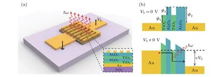
Fig. 1. (a) Schematic diagram of the device. The inset shows a side view of active region (unscaled), and contains, from bottom to top, a silica substrate,a square Au bottom electrode,alternative insulator layers,and an Au grating. The 50-nm-thick gratings are fabricated onto the bottom electrode with a 4-nm-thick tunnel barrier of TiO2&Al2O3 grown in between. (b)Energy band diagram of multilayer tunnel junction with zero and positive bias,with Φi (i=1,2,3)denoting barrier height,Vb applied voltage,and ˉhω light emission.
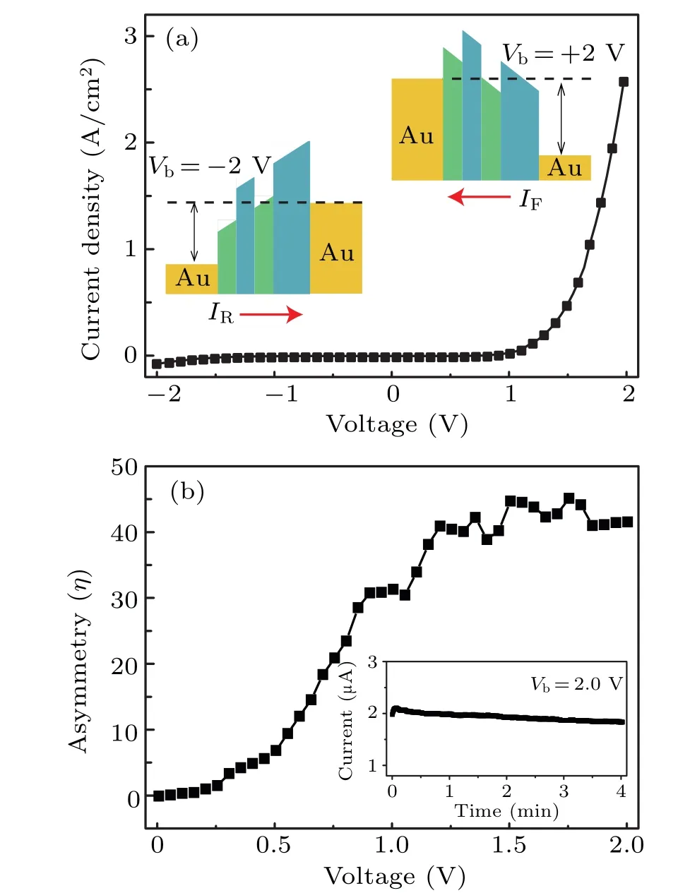
Fig.2.(a)Current-voltage characteristic curve of connected plasmonic grating device with a tunneling gap, where insets show energy band diagrams of multilayer tunneling junction with a negative or positive bias applied to top Au electrode. (b)Asymmetry(η =|IF/IR|)versus bias voltage for the MIM tunnel diode,where inset displays time trace of tunneling current at a constant bias of Vb=2.0 V with tunnel junction size being 60μm2.
The tunneling current of our device is determined by both the amplitude and the direction of the applied voltage since there are multiple insulators with different electron affinities in the tunnel barrier. The characteristic of current density(J)as a function of the applied voltage is shown in Fig.2(a). A pronounced asymmetry appears when the direction of injection electrons is reversed. The inset of Fig. 2(a) presents the energy band diagram with negative and positive voltage. When applying a positive bias voltage of +2 V to the top Au electrode, the width of the TiO2&Al2O3tunnel barrier is smaller than that when applying a negative bias of-2 V. Hence, the positive current density is greater than the negative one at the MIM tunnel junction. In the following,we always use a positive bias in the LEIT measurements since the intensity of emission photons depends linearly on the amplitude of the tunnel current.[20]Supporting information figure S2 also shows that the tunneling current increases linearly with the augment of area of the junction.
We now come to study the asymmetry of the currentversusvoltage(I-V)curve and the stability of the tunnel junctions. The asymmetry of theI-Vcurve is defined as the forward current divided by the reverse current (η=|IF/IR|),which presents the characterization of rectification for a tunnel MIM diode. Figure 2(b)shows that the value of asymmetry is related to the value of applied voltage. The asymmetry value of the tunnel junction reaches 45 when|Vb|=2 V.The inset of Fig. 2(b) shows the time trace of the tunneling current of the MIM junction with a junction size of 60μm2at a bias voltage of 2.0 V. The tunneling current keeps stable during the measurement, guaranteeing key feature required in further applications (e.g., optoelectronic circuits). Stabler devices can be achieved by packaging the final device or utilizing the transferred top Au nanostructure(electrodes).[38]

Fig. 3. (a) Reflection spectra of grating under parallel (red) and perpendicular (black) excitation. Inset shows scanning electron microscope image of the grating. It has a duty cycle of 0.5 and a period of 700 nm. Scale bar: 1μm. (b)Simulated reflection spectra of the grating under parallel(red)and perpendicular excitation. The inset shows the electric field distribution under the resonance condition with a wavelength of 750 nm. (c)EL spectra of the grating for various applied voltages. The inset shows the I-V curve of the device. (d)Image of light emitted from the grating at a constant bias of Vb=3.0 V.The CCD exposure time is 3 s. The right panels indicate the intensity profiles along the major axis and minor axis of the EL image,corresponding to the dashed line on the left panel.
The optical characterization of the tunneling device and the emission spectra of the LEIT source are determined by the resonance properties of the grating. The reflection spectra are measured in the home-built microscope (for details, see supporting information Fig. S3). Considering that the plasmon resonance has a smaller loss in the near-infrared region,[37]the grating is designed with a duty cycle of 0.5 and a period of 700 nm.Figure 3(a)shows the reflection spectra from the grating under perpendicular and parallel polarization. The grating shows a strong polarization response, an apparent reflection dip at 770 nm shows up under perpendicular polarization.The polarization dependence of EL spectrum presents a similar behavior,with the emitted photon polarized perpendicular to the grating (supporting information, Fig. S6).The inset of Fig. 3(a) shows the scanning electron microscopy images of the same devices. Numerical simulations of the grating nanostructure are in good agreement with the experimental result as shown in Fig. 3(b). The inset shows a side view of the electric field distribution of a grating at the resonant wavelength.High enhancement of the electric field is confined in the tunnel junction and at the top edge of the grating,which conduces to improving the efficiency of LEIT device.
Next,we explore the properties of the emission light from the electrically driven grating. We use two tungsten probes connected with a sourcemeter to apply the bias voltage to the device. Light emission from the tunneling junction is collected by a long working distance objective (Olympus, 50×,NA=0.5)and then recorded by a CCD camera or by a spectrometer(for details,see Methods).All measurements are conducted at room temperature. Figure 3(c) shows the emission spectra with various bias voltages, the intensity of EL peak becomes stronger with voltage increasing. The peak position of EL spectrum is 728 nm,which fits well with the reflection spectrum. We note that the drop of the EL spectrum at about 820 nm is not caused by the experimental collection system.It may be due to the lower electric field enhancement in the tunnel junction and at the top edge of the grating,corresponding to a weak radiation efficiency at the dip (~840 nm) in the reflection spectrum in Fig. 3(b) (also see supporting information Fig. S7). The inset of Fig. 3(c) shows the correspondingI-Vcurves of the same device. Figure 3(d) shows the direct imaging of light emitted from gratings at a constant bias voltage ofVb=3.0 V.The intensity of the emission spot is uniform, which shows that the tunneling electrons uniformly pass through the barrier of the MIM junction. The right panels show that the intensity profiles along the different axes of the tunnel source, and there appear only small fluctuations from different positions. Supporting information Fig.S5 shows the photon emission from a planar MIM tunnel junction, and the emitted photons are observed only from the edges of the top electrode. The external conversion efficiency of the electronto-photon of the light source is estimated at about 3.8×10⁻⁶atVb=3.0 V,following the same procedure as in our previous work.[20]
4. Conclusions
In this work, we demonstrate electrically driven plasmonic gratings based on a multilayer tunneling barrier grown by ALD,where the source shows stable and uniform emission characteristics. Four insulator layers are utilized to fabricate the MIM tunneling sources for the first time. It shows that the tunneling probability of one electron is dependent on the injection direction due to the utilization of the multiple insulators with different electron affinities in one tunnel barrier.The tunneling probability of the electrons from the bottom Au electrode is much higher than that from the top grating. The problem of poor stability of the ultrathin insulator layer grown by ALD in the MIM tunnel source is solved by utilizing multilayer barriers. According to Ref.[39],the resonant electron tunneling based on multilayer barriers may happen and will further enhance the efficiency.[39]Our work paves the way for fabricating a stabler and efficient subwavelength LEIT device,which is of potential significance in implmenting the on-chip optical communication,biosensing,and photodetection.
Acknowledgements
Project supported by the National Natural Science Foundation of China (Grant Nos. 12004222 and 91850207),the National Key Research and Development Program of China(Grant Nos.2017YFA0303504 and 2017YFA0205800),the Fundamental Research Funds for the Central Universities, China, the Strategic Priority Research Program of Chinese Academy of Sciences (Grant No. XDB30000000),and the Postdoctoral Science Foundation of China (Grant No.2020M682223).
猜你喜歡
青年文學(xué)家(2023年2期)2023-05-30 21:59:18
青年文學(xué)家(2023年9期)2023-05-30 16:17:46
青年文學(xué)家(2022年5期)2022-03-25 13:17:27
智能制造(2021年4期)2021-11-14 18:56:41
綠色天府(2021年9期)2021-10-15 06:16:32
無(wú)錫商業(yè)職業(yè)技術(shù)學(xué)院學(xué)報(bào)(2019年4期)2019-09-04 11:07:24
Chinese Physics B(2019年2期)2019-02-25 07:22:56
知識(shí)經(jīng)濟(jì)·中國(guó)直銷(2016年7期)2016-11-07 09:36:31
股市動(dòng)態(tài)分析(2015年29期)2015-09-10 07:22:44
當(dāng)代音樂(lè)(下旬刊)(2015年5期)2015-05-30 05:21:05

- Chinese Physics B的其它文章
- Role of compositional changes on thermal,magnetic,and mechanical properties of Fe–P–C-based amorphous alloys
- Substrate tuned reconstructed polymerization of naphthalocyanine on Ag(110)
- Anti-PT-symmetric Kerr gyroscope
- Information flow between stock markets:A Koopman decomposition approach
- Cascading failures of overload behaviors using a new coupled network model between edges
- High efficiency ETM-free perovskite cell composed of CuSCN and increasing gradient CH3NH3PbI3