
Improving the surface flashover performance of epoxy resin by plasma treatment: a comparison of fluorination and silicon deposition under different modes
2021-11-30 08:28:44JiyuanYAN閆紀(jì)源GuishuLIANG梁貴書HongliangLIAN廉洪亮YanzeSONG宋巖澤HaoouRUAN阮浩鷗QijunDUAN段祺君andQingXIE謝慶
Plasma Science and Technology 2021年11期
關(guān)鍵詞:洪亮
Jiyuan YAN (閆紀(jì)源), Guishu LIANG (梁貴書), Hongliang LIAN (廉洪亮),Yanze SONG (宋巖澤), Haoou RUAN (阮浩鷗), Qijun DUAN (段祺君) and Qing XIE (謝慶),?
1 State Key Laboratory of Alternate Electrical Power System with Renewable Energy Sources,North China Electric Power University, Beijing 102206, People’s Republic of China
2 Electrical and Electronic Engineering of North China Electric Power University, Baoding 071003,People’s Republic of China
Abstract This work treats the Al2O3-ER sample surface using dielectric barrier discharge fluorination(DBDF), DBD silicon deposition (DBD-Si), atmospheric-pressure plasma jet fluorination (APPJ-F) and APPJ silicon deposition (APPJ-Si).By comparing the surface morphology, chemical components and electrical parameters,the diverse mechanisms of different plasma modification methods used to improve flashover performance are revealed.The results show that the flashover voltage of the DBDF samples is the largest (increased by 21.2% at most), while the APPJ-F method has the worst promotion effect.The flashover voltage of the APPJ-Si samples decreases sharply when treatment time exceeds 180 s, but the promotion effect outperforms the DBD-Si method during a short modified time.For the mechanism explanation, firstly, plasma fluorination improves the surface roughness and introduces shallow traps by etching the surface and grafting fluorine-containing groups,while plasma silicon deposition reduces the surface roughness and introduces a large number of shallow traps by coating SiOx film.Furthermore,the reaction of the DBD method is more violent,while the homogeneity of the APPJ modification is better.These characteristics influence the effects of fluorination and silicon deposition.Finally, increasing the surface roughness and introducing shallow traps accelerates surface charge dissipation and inhibits flashover, but too many shallow traps greatly increase the dissipated rate and facilitate surface flashover instead.
Keywords: surface charge, flashover voltage, dielectric barrier discharge, atmospheric-pressure plasma jet, plasma fluorination, plasma silicon deposition
1.Introduction
The rapid development of high-voltage direct current (HVDC)power transmission systems puts forward higher requirements for the electrical equipment’s insulation performance [1, 2].Al2O3-filled epoxy resin (Al2O3-ER) spacers are employed in gas insulated transmission lines (GILs) because of their good mechanical and electrical properties, but the surface flashover occurring on the spacers limits the further promotion of GILs[3, 4].Previous theoretical research indicates that the flashover under a DC electric field is affected by surface charges that accumulate on gas–solid interfaces [5], and the surface charge motion characteristics are mainly related to the surface roughness[6],trap distribution[7,8],surface conductivity and volume conductivity [9, 10].As these parameters are affected by the physicochemical characteristics of the surface, many methods have been proposed which can change the physical morphology and chemical elements of the surface of the insulating materials and improve the insulation quality.Xie et al [11] studied the relation between surface morphology and flashover performance of Al2O3-ER after discharge aging.Zhang et al [12] addressed the fact that the rough treatment of the insulating material’s surface can restrain surface charge accumulation and improve surface flashover performance.An et al[13]treated epoxy resins with direct fluorination to change surface conductivity and improve flashover voltage.Li et al [14] suppressed charge injection from the electrode using a Cr2O3-sputtered method.
Plasma surface treatment technology is widely used as a novel method to enhance the surface-insulating performance of materials without affecting the internal structures of the material [15–17].The typical methods used to generate plasma are the dielectric barrier discharge (DBD) and atmospheric-pressure plasma jet (APPJ) [18, 19].In addition,plasma fluorination and silicon deposition are effective methods used to improve insulation performance.For plasma fluorination,Zhan et al[20]utilized DBD plasma fluorination to increase the direct current and alter the current flashover voltage of an Al2O3-ER sample.Chen et al [21] applied He/CF4APPJ treatment to enhance flashover-withstanding characteristics of Al2O3-ER.For plasma silicon deposition,Shao et al[22,23]used tetraethyl orthosilicate(TEOS)as the precursor to modify an Al2O3-ER sample.They studied the effects of the electrode structure and the oxygen content on the electrical parameters.They also reported that plasma silicon deposition can improve the electrical performance of fluorinated ethylene propylene [24].
For plasma modification,there are different combinations of the electrode structure and the precursor that can be used.But most research focused on a single method to improve insulation performance,and they did not compare the various methods.Zhang et al[25]treated Al2O3-ER samples as DBD etching and DBD deposition, and the surface charge dissipation was compared.Kostov et al [26] compared the effects of DBD and APPJ on the polymer’s surface morphology,but they only used a single gas to generate the plasma.Previous theoretical research indicates that the different plasma modifications have distinctive influences on surface morphology, chemical components, surface charge dissipation, flashover and so on.The comparison between the various methods used to study the improvements is helpful in revealing the inherent law of suppression of flashover and regulation of surface charge.In this paper, two types of plasma discharge forms (DBD and APPJ) and two kinds of element modification methods (fluorination and silicon deposition) are combined to treat the Al2O3-ER sample surface.By measuring the surface morphology, chemical elements and surface electrical parameters before and after treatment, the enhancing mechanism of the flashover voltage using the different modification methods is compared and analyzed.
2.Experimental methods
2.1.Sample preparation
The Al2O3-ER samples used in this experiment are prepared by our team.The matrix(E-51 type bisphenol A epoxy resin),curing agent (methyl-tetrahydro phthalic anhydride type,MTHPA), accelerator (2, 4, 6-tri (dimethylaminomethyl)phenol, DMP30) are manufactured by Shanghai Resin Factory.The Al2O3-fillers are manufactured by Shanghai Chaowei Nano Technology Co.Ltd, and the particle diameter range is from 50 μm to 100 μm.The relative mass ratio of the matrix, curing agent, accelerator and filler is 100:80:1:300,and the preparation process used to prepare the Al2O3-ER samples is displayed in figure 1.After stirring, deaerating,injecting and curing,circular samples of 40 mm diameter and 15 mm thickness are prepared.The Al2O3fillers are uniformly distributed using this process, which can avoid the effects of fillers on experiment results [27].Before treatment, all samples are cleaned in an ultrasonic cleaner with deionized water for 30 min, and then the sample surface is rinsed with absolute ethanol.Finally,the cleaned samples are dried in a drying oven at 50°C and dried for 10 h.
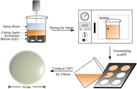
Figure 1.The preparation flow chart of the Al2O3-ER sample.
2.2.Plasma modification
The modification platforms of the DBD and APPJ are shown in figure 2.Both platforms are composed of an electrical circuit part and a gas channel part.The electrical circuit part of the DBD modification platform, shown in figure 2(a),consists of a high-frequency high-voltage power supply(center frequency 50 kHz, output voltage: 0–20 kV), a DBD reactor and a capacitor with 0.1 μF.The DBD reactor includes two circular metal-plate electrodes.One is connected to the power supply and the other is in series with a grounded capacitor.The untreated sample is placed in a quartz glass container, and a quartz glass sheet is placed on the top of the container.The discharge gap in this DBD reactor is 6 mm.The voltage waveforms of the capacitor and the power supply are captured by an oscilloscope (Tektronix DPO 2002B),which can obtain the Lissajous figures and calculate the discharge power.The gas channel is separated into the fluorination part and the silicon deposition part.Argon (Ar) and tetrafluoromethane(CF4)are passed into the DBD reactor and the flow rates are controlled by their respective mass flowmeters, which constituted the fluorination part.The silicon deposition part contains two bottles of Ar, the mass flowmeters and the TEOS.One bottle of Ar is directly introduced into the DBD reactor, the other is firstly pumped into the bubbling bottle containing TEOS, and then passed into the DBD reactor.To fully mix the TEOS and Ar, the bubbling bottle is heated to 70 °C.The flow rates of all gases and output voltage parameters are shown in table 1.It is worth mentioning that fluorination and silicon deposition was not carried out at the same time.
The composition of the APPJ modification platform,shown in figure 2(b), is similar to that of the DBD platform,except that the reactor is replaced by a plasma jet array gun.This gun had a high-voltage unit,a grounded unit,four quartz glass tubes and other components used for fixing or insulating.Both the high-voltage unit and the grounded unit are metal cylinders with four holes,and the aperture of each hole matches the glass tubes.One cylinder is connected to the high-voltage high-frequency power supply, while the other cylinder is grounded.Four glass tubes are passed through these metal cylinders and attached to the gas channel.Each tube is equipped with a mass flowmeter.The distance between the jet gun and untreated sample is set to 20 mm,and the sample is placed on a rotating platform to ensure the uniformity of treatment.
All the untreated Al2O3-ER samples are separated into five groups: untreated samples (UT), DBD fluorination samples (DBD-F), DBD silicon deposition (DBD-Si), APPJ fluorination samples (APPJ-F) and APPJ silicon deposition(APPJ-Si).The treatment time is set to 60 s, 120 s, 180 s,240 s and 300 s.Table 1 shows the gas flow rates and the discharge parameters for all the modification methods.During the plasma fluorination, we found that the plasma plume is orange, the discharge is violent, and the discharge power is higher.It is worth mentioning that long duration and continuous plasma fluorination sometimes scorch the sample surface.By comparison, the plasma plume of plasma silicon deposition is lavender, and the discharge is moderate.
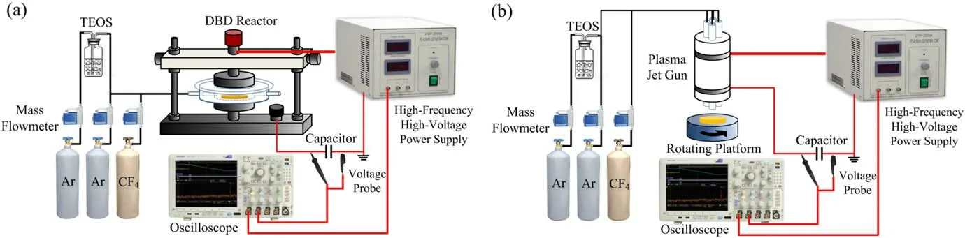
Figure 2.Schematic diagrams of the plasma modification platform: (a) DBD platform, (b) APPJ platform.
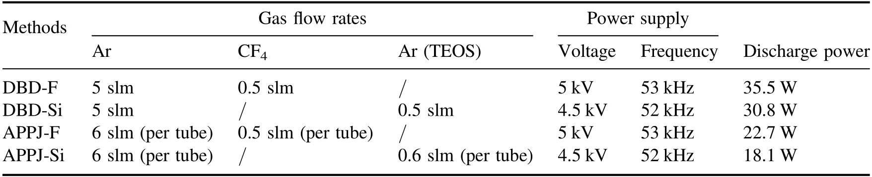
Table 1.Parameters of all the plasma modification methods.
2.3.Characterization
For all the samples, the surface physical morphology, chemical elements and surface electrical properties are measured.The microscopic morphology is observed using scanning electron microscopy (SEM, Hitachi S4800).The surface roughness is measured using a surface profilometer (Bruker,model Contour GTK).For each sample, the roughness is measured at five points and the average of these five values represents the surface roughness of the sample.The compositions of the chemical elements are estimated using x-ray photoelectron spectroscopy (XPS, Thermo Scientific Escalab 250Xi).The surface conductivities of all the samples are measured using an SM7110 high-resistance meter.
Figure 3 shows the platforms of the surface potential and surface flashover voltage measurements.As seen in figure 3(a), the surface potential measurement platform consists of a negative HVDC power supply (0 to ?50 kV), a stainless steel charging pin, a 2D control device, an electrostatic potentiometer (Trek P0865), a capacitive probe (Trek 6000B), an acquisition card and a computer.During the surface potential decay experiment,the sample is placed on a grounded aluminum plate and 5 mm below the charging pin.A voltage of ?7 kV is applied to the charging pin for 60 s to generate a corona discharge.After charging, the pin is removed and the capacitive probe is moved 2 mm above the sample.Finally, the surface potential data are stored in the computer through an electrostatic potentiometer and an acquisition card.The experiment is carried out at 25 °C and humidity of 30%.
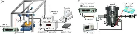
Figure 3.The measurement platform of surface electrical performance: (a) surface potential decay, (b) surface flashover voltage.
The flashover voltage test platform,shown in figure 3(b),includes a negative HVDC power supply (0 to ?50 kV), a 10 MΩ protection resistance, a stainless cavity with two adjustable needle electrodes and a lifting platform to place the sample, a high-voltage probe (Tektronix, P6015A) and an oscilloscope (Tektronix DPO 2002B).It is worth mentioning that in our previous work [11], we studied the influence of different electrodes on the flashover voltage of the sample.We found that the fluctuation of the flashover voltage under needle–needle electrodes is the smallest.Therefore, we have chosen the needle–needle electrodes to reduce measurement error.When testing the surface flashover voltage, the gap between two needle electrodes is 7 mm, and the sample is closely attached to the electrodes.The negative voltage is increased at the rate of 0.5 kV s?1until the flashover occurs,and then the flashover voltage is measured using a highvoltage probe and recorded using an oscilloscope.Each sample is tested ten times, and the average value is taken as the sample’s flashover voltage.The experiment temperature and humidity are the same as the flashover test.
3.Results
3.1.Surface morphology
While different treatment times have little effect on the surface morphology of samples, different treatment methods have a significant influence on the surface morphology.Figure 4 displays the SEM and surface roughness images of samples that were untreated and treated for 180 s, and the relation between surface morphology and treatment time is shown in figure 5.It is found that a lot of gullies and bulges appear on the surface of the sample,regardless of the DBD-F or the APPJ-F, and the values of Ra increase with treatment times.Furthermore,the sample surface modified by the DBDF is rougher than that treated by the APPJ-F.By comparison,the gullies and bulges of the surface are reduced after two types of silicon deposition, and Ra is also decreased.While the APPJ-Si treated sample surfaces were smoother,some flat regions also appeared in the DBD-Si treated samples.Based on these experiments, it is inferred that plasma fluorination mainly etches the material surface, while plasma silicon deposition primarily deposits thin films on the material surface.Moreover, the effects of the DBD and the APPJ treatment on samples are different.
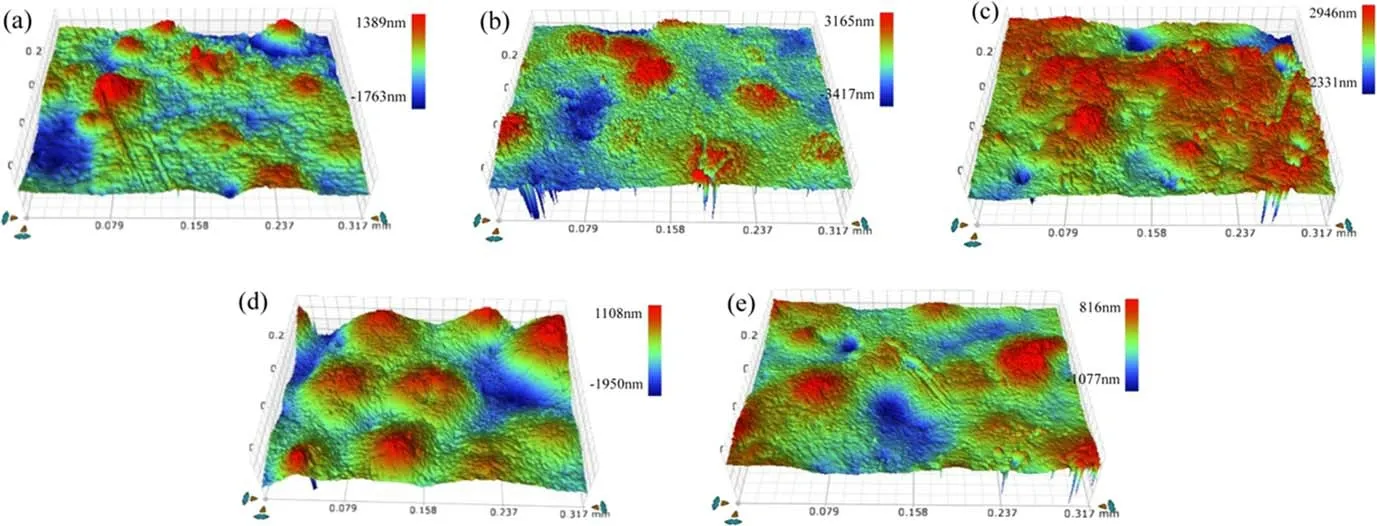
Figure 4.The surface morphology images with different treatment methods:(a)untreated,(b)DBD-F180s,(c)APPJ-F180s,(d)DBD-Si180s,(e) APPJ-Si180s.
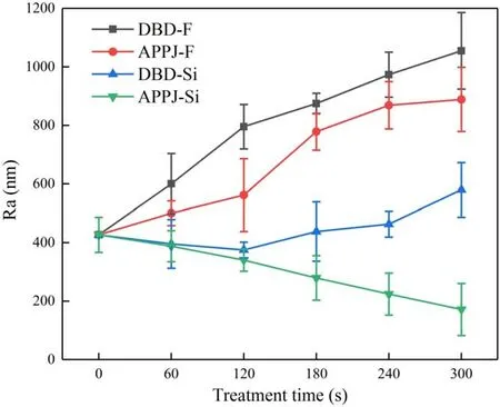
Figure 5.Surface roughness (Ra) with different treatment methods.
To confirm this assumption, figure 6 shows the 100 μm SEM testing results from the samples before and after plasma modification.It is found that the Al2O3-ER surface is etched after plasma fluorination, and the Al2O3fillers are gradually exposed.These fillers increase the surface roughness.Besides,the etching effect of the DBD-F is clearly better than that of the APPJ-F, which causes more fillers to be exposed by DBD-F,and the surface roughness is greater.By comparison,a thin film formed on the material surface after plasma silicon deposition.The distribution of this film is non-uniform in the DBD-Si, while the film formed by the APPJ-Si covers the original defects on the surface more evenly.Magnification of the SEM images of the two plasma silicon deposition methods,seen in figure 7, shows the coral-like particles are deposited on the sample surface,but the uniformity of the DBD-Si film is worse than that of the APPJ-Si film.
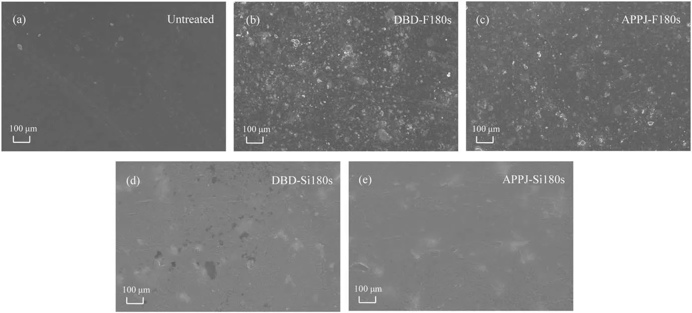
Figure 6.The SEM images with different treatment methods:(a)untreated,(b)DBD-F180s,(c)APPJ-F180s,(d)DBD-Si180s,(e)APPJ-Si180s.
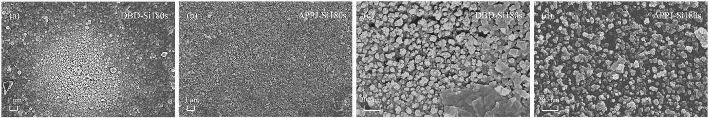
Figure 7.The SEM images of DBD-Si and APPJ-Si samples at high magnification:(a)DBD-Si at 1 μm,(b)APPJ-Si at 1 μm,(c)DBD-Si at 200 nm, (d) APPJ-Si at 200 nm.
3.2.Chemical components
The XPS spectra of the sample surface with the DBD and APPJ fluorination are shown in figure 8.On the basis of these spectra,the relative element contents on the sample surface before and after treatment are listed in table 2.Apparently, the fluorine content increases significantly after DBD-F treatment, while the APPJ-F method introduces less fluorine.The APPF-F experimental data are similar to the results in [21].It is also found that the oxygen content undergoes little change before and after plasma fluorination, but the treatment time has a great influence on the content of carbon and fluorine elements.Combined with the test results of the surface morphology, it is considered that plasma fluorination will seriously etch the material surface and the inner alumina filler will be exposed.On the other hand, the CFxand fluorine content produced by the decomposition of CF4is so low that the thin film cannot form.Therefore,after plasma fluorination,the fluorine is introduced to the epoxy resin sample by grafting and bonding [28].Besides,since the APPJ is carried out in the air environment, some oxygen elements are involved in the reaction,which will reduce the relative content of the F elements.
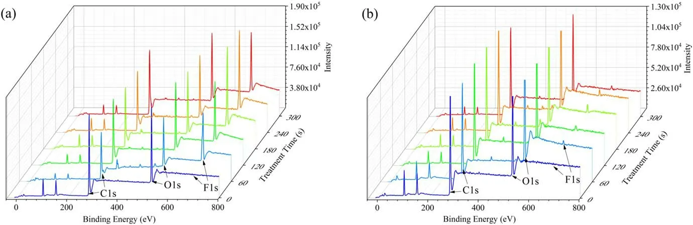
Figure 8.The XPS spectra of samples treated by plasma fluorination: (a) DBD-F, (b) APPJ-F.
To further confirm the surface chemical bonds of plasma fluorinated samples, the C 1s XPS spectra of untreated, DBDF180 and APPJ-F180 samples are shown in figure 9.It can be seen that C–F bonds and CFxgroups are formed on the surfaces of the samples after plasma fluorination.This is because the bond energies of C–F (485 kJ mol?1) and H–F (565 kJ mol?1) are much larger than those of F–F (153 kJ mol?1) and C–H(414 kJ mol?1).When the sample is plasma fluorinated,energetic particles generated by discharge will collide with CF4and the Al2O3-ER surface,some of the free F atoms in CF4gas will bond with free H atoms to form HF, and other free F atoms will combine with free radicals that appear on the sample to form a stable C–F bond [29].
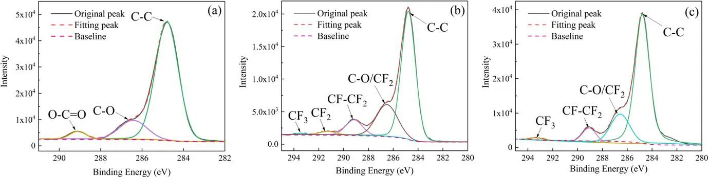
Figure 9.C 1s XPS spectra of samples before and after plasma fluorination: (a) untreated, (b) DBD-F, (c) APPJ-F.
Furthermore, table 3 lists the content ratios of chemical bonds before and after plasma fluorination.As seen in table 3 and figure 9,new groups such as C–CF2(286.6 eV),CF–CF2(289.3 eV) and CF3(293.0 eV) appear after the APPJ-F treatment, while the DBD-F samples not only have these groups,but also find CF2(291.0 eV)groups.Considering that the DBD-F samples have a higher fluorine content than the APPJ-F samples, it means that the fluorination effect of the DBD-F method is better than that of the APPJ-F method.Besides, figure 10 shows the F 1s XPS spectrum of the Al2O3-ER surface after the DBD-F, and the metal fluoride peak (685 eV) and organic fluoride peak (688 eV) are found.According to [30, 31], HF produced by plasma fluorination reacts with the Al2O3filler to form AlOFxgroups.This reaction also demonstrates that plasma fluorination etches the Al2O3-ER surface and exposes the filler, and these exposed fillers promote the grafting of fluorine.In summary,the main reactions of plasma fluorination are elucidated in equation(1).
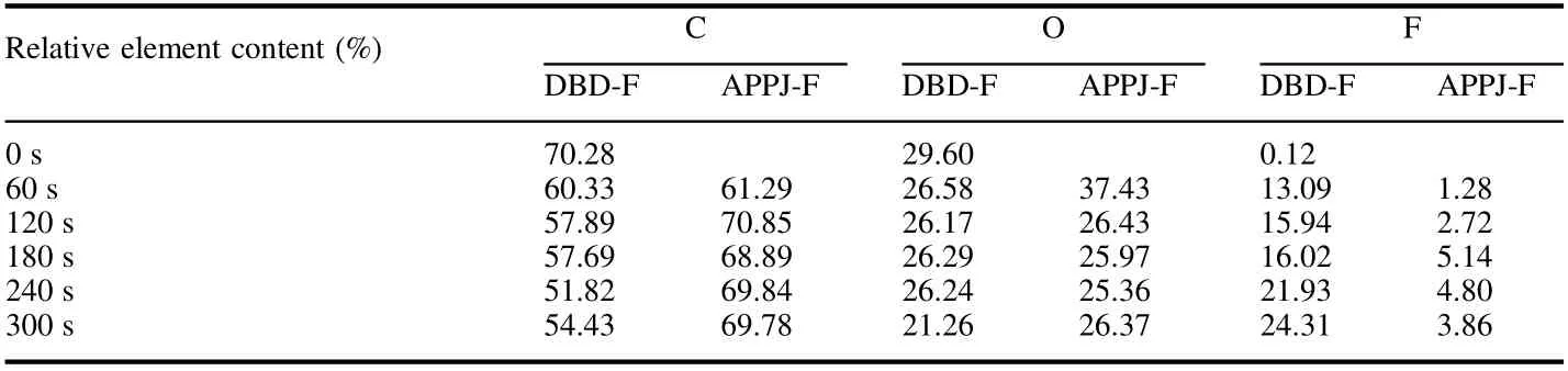
Table 2.The relative element contents of the sample surface before and after plasma fluorination treatments.
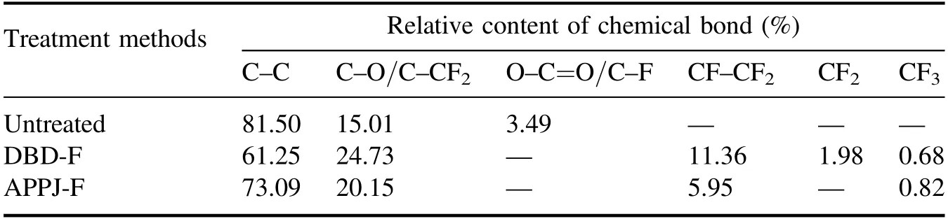
Table 3.Ratios of chemical bond contents before and after plasma fluorination.
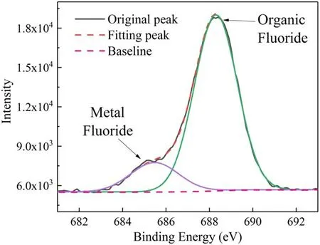
Figure 10.The F 1s XPS spectrum of the Al2O3-ER sample after DBD-F.
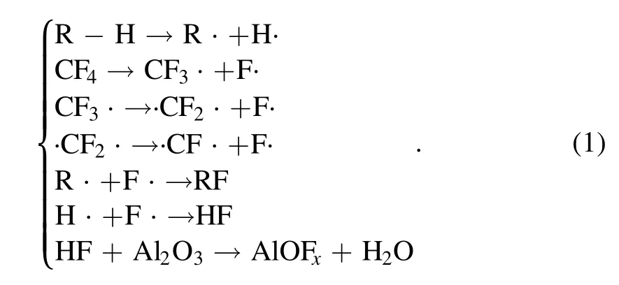
Similarly, XPS spectra of samples after two types of plasma silicon deposition are shown in figure 11.Because micron Al2O3fillers are pretreated with silane coupling agents to prevent filler aggregation, untreated samples also contain some silicon elements.However, both the plasma silicon deposition modifications significantly increase the silicon content.The relative element contents on the material surface at different treatment times are listed in table 4.Compared to plasma fluorination, the oxygen and silicon contents increase remarkably after plasma silicon deposition.This is because the plasma silicon deposition method utilizes TEOS as a precursor.When the film is depositing, a two-step reaction occurs as follows [32].Firstly, TEOS collides with the highenergy electrons in the plasma to produce Si(OH)xas an active intermediate, seen in equation (2).Then, polycondensation occurs between the gaseous phase Si(OH)xgroups and Si-OH groups on the material surface to produce a large number of Si-O-Si groups, seen in equation (3).Furthermore, the long-duration APPJ will scorch the sample surface,which will increases the C elements and decrease the relative content of the Si elements:
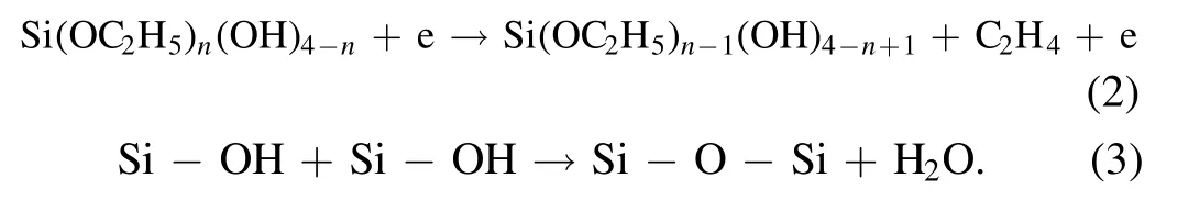
Figure 11.The XPS spectra of samples treated by plasma silicon deposition: (a) DBD-Si, (b) APPJ-Si.
Table 4.Relative element contents of the sample surface before and after plasma silicon deposition treatments.
In combination with the test results of the surface morphology, it is found that the reaction mechanism of plasma fluorination,which makes the fluorine directly bond to the Al2O3-ER surface, is different with plasma silicon deposition.The latter method will form a dense silicon oxide thin film, which will be deposited on the Al2O3-ER surface.On the one hand, the plasma silicon deposition method can reduce the surface roughness of materials; on the other hand,this method can change the distribution of the chemical elements on the material surface.Figure 12 displays the Si 2p XPS spectra of untreated, DBD-Si180 and APPJ-Si180 samples.As seen in this figure, the Si(-O2) (102.2 eV),Si(-O3) (102.8 eV) and Si(-O4) (103.4 eV) peaks appear in these three spectra.According to these spectra, the relative contents of silicon-containing groups are listed in table 5.Because the untreated Al2O3-ER sample surface is affected by the silane coupling agent, a large number of Si(-O2) groups and a small number of Si(-O3) and Si(-O4) groups are detected.Nonetheless, the relative content of Si(-O3) and Si(-O4) groups on the sample is greatly increased by the plasma silicon deposition,and the content of Si(-O4)groups is much larger after the APPJ-Si treatment.The explanation is as follows: except for the plasma silicon deposition, which can synthesize Si-O-Si thin film,as mentioned above,the DBD-Si treatment in this paper is carried out in a reactor filled with Ar.But the APPJ-Si method is conducted in air, which causes water molecules and oxygen to participate in the reaction together, thus increasing the oxygen content on the sample surface.
Figure 12.Si 2p XPS spectra of samples before and after plasma silicon deposition: (a) untreated, (b) DBD-Si, (c) APPJ-Si.
3.3.Flashover voltage
The DC flashover voltage test results for all the samples are shown in figure 13.As can be seen, the flashover voltages of all the plasma-modified samples are higher than those of the untreated samples (9.45 kV).Among these, the best method to enhance the samples’ flashover voltage is the DBD-F treatment, which increases the flashover voltage by 21.2%(11.45 kV).Then, the flashover voltage of all the samples roughly increases first and then decreases as the treatment time increases, and the flashover voltage of the APPJ-Si sample decreases sharply when the treatment time exceeds180 s, which drops at most by 11% (from 11.28 kV to 10.03 kV).The flashover voltage of treated samples over a short processing time can be ranked as: DBD-F >APPJSi>DBD-Si>APPJ-F,while the enhanced performance of the treated sample flashover voltage over a long processing time can be ranked as:DBD-F > DBD-Si>APPJ-F > APPJ-Si.A detailed explanation of the effect of treatment methods on flashover voltage is given in section 4.
Figure 13.The flashover voltages of all the samples.
Table 5.Ratios of chemical bond contents before and after plasma silicon deposition.
3.4.Surface potential decay and trap level distribution
Previous theoretical research indicates that, for an insulating material, there is a correlation between the surface flashover and the surface charge dissipation, and this dissipation can be characterized by surface potential decay [33].Figure 14 shows the dependence of the surface potential and decay time for all the samples.Note that the surface potential decay rate of the plasma fluorinated samples is slower than that of the plasma silicon deposition.In particular,the APPJ-Si method reduces the sample surface potential to the initial 10% after 1800 s.Moreover,regardless of the modification method,the surface potential decay rate gradually increases with the modification time.However,the decay rates of all the plasma silicon deposited samples are faster than those of the untreated samples, while the decay rates of the plasma fluorinated samples treated for a short time are lower than those of the unmodified samples.
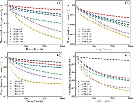
Figure 14.The surface potential decay curves of all the samples: (a) DBD-F, (b) APPJ-F, (c) DBD-Si, (d) APPJ-Si.
The surface charge dissipation of insulating materials depends on the distribution of the trap energy levels.In general, the surface potential decay curves of insulating materials can be fitted into a double exponential function, as in equation (4) [34]:
where t represents the decay time,φs(t)represents the surface potential, and A, B, m and n represent fitting coefficients.On the basis of the isothermal surface potential decay (ISPD)theory, the trap level ETand trap density Qsof insulating material are shown in equations (5) and (6) [35]:
where kBrepresents Boltzmann’s constant, T represents the absolute temperature, v represents the attempted escape frequency, e represents the charge of an electron, L represents material thickness, and ε0and εrrepresent vacuum permittivity and relative permittivity, respectively.Calculated using the ISPD theory, the trap distribution characteristic curves of all the samples are shown in figure 15.Note that both kinds of plasma silicon deposition methods decrease the trap depths of the samples.However, the DBD-F method is not effective enough to reduce the trap depth, and the trap depth is almost unchanged after APPJ-F.According to the experimental results of chemical components, the trap distribution of the sample surface is closely related to the change in surface chemical elements.The plasma fluorination method shallows the trap level by introducing fluorinated groups [25].The APPJ-F method in this paper only introduces a few fluorinated groups, which has little influence on trap distribution.The DBD-F method over a short processing time cannot form a uniform fluorination layer,which causes only a few shallow traps to be introduced.Instead, using plasma silicon deposition methods, a lot of SiOxand Si-O-Si groups are deposited on the sample surface and a dense thin film is formed.The following shallow traps are introduced and change the trap distribution of the sample surface.
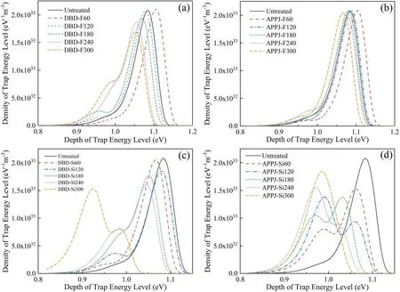
Figure 15.The trap level distribution of all the samples: (a) DBD-F, (b) APPJ-F, (c) DBD-Si, (d) APPJ-Si.
3.5.Surface conductivity
The surface conductivities of all the samples are shown in figure 16.It can be seen that the surface conductivities of modified samples are higher than that of the untreated sample (3.11 ×10?18S),and they increase with the treatment time.Furthermore,the plasma silicon deposition methods can significantly improve the surface conductivity of the Al2O3-ER samples, while the promotion effect of the plasma fluorination methods is not obvious.The variation trend of the surface conductivity is almost the same as that of the surface potential decay and trap level distribution,which can verify the reliability of all the test results.
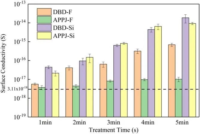
Figure 16.The surface conductivities of all the samples.
4.Discussion
4.1.Comparison of different plasma modifications
As seen from the surface morphology and chemical component results,the DBD-F treatment,compared with the APPJ-F method, not only etches the Al2O3-ER surface more severely, but also grafts more fluorine elements into the surface.This is because the electrode structure of the DBD overlaps the discharge region and the treatment region,which causes the sample surface not only to react with the active particles, but also to be bombarded with high-energy ultraviolet photons and a large number of charged particles [36].So the DBD has a more vigorous reaction.In comparison,the electrode structure of the APPJ separates the discharge region and treatment region, which significantly weakens the influence of high-energy ultraviolet photons and charged particles on the sample surface.Therefore,the sample surface is mainly affected by active substances during APPJ treatment, and the reaction is moderate [26].In addition, the fluorine is introduced to the Al2O3-ER sample by grafting and injection during plasma fluorination.This means that the etching degree of the sample surface, named surface roughness,increases with the treatment time.
However,the experimental results of the DBD and APPJ silicon deposition seem to contradict the aforementioned explanations.This is because both the DBD-Si and APPJ-Si methods can effectively decompose TEOS to form compact SiOxfilm,which deposits on the sample surface.Furthermore,the electrode structure of the APPJ is more flexible than that of the DBD,which can deposit the uniform film and decrease the surface roughness.The uneven discharge of the DBD will produce inhomogeneous films, which causes the surface roughness to increase a little.
4.2.Effect of different modification methods on surface flashover of material
As shown in figure 12, the flashover voltage of the APPJ-F treated samples is relatively the lowest.The APPJ-F method boosts the surface roughness of the sample and slightly increases the surface potential decay rate.References[12,36]considered that the promotion of surface roughness decreased the distance of the surface charge migration,which meant that more surface charges were absorbed during migration.Thus,the surface potential decay rate is promoted,and the flashover is suppressed to some degree.However, the APPJ-F method has little influence on the sample surface element content,trap distribution and surface conductivity, so it has a limited inhibitory effect on flashover.
As another method of plasma fluorination, the DBD-F treatment increases the sample flashover voltage the most.This paper considered that the DBD-F method promotes the flashover performance due to the changes in physical morphology and chemical composition.On the one hand,the DBD-F method increases the sample surface roughness, and the enhancing mechanism on surface electrical properties is the same as that of the APPJ-F.But the DBD-F modification grafts a large number of fluorine-containing groups, resulting in shallow traps appearing on the sample surface.Due to these shallow traps, surface charges are easier to detrap and less susceptible to accumulation, which weakens the ability of surface charges to distort the electric field and further enhance the flashover voltage.
Although both plasma silicon deposition methods change the physical morphology and chemical composition of the sample,their effect on the flashover voltage is inferior to that of the DBD-F method.Particularly prolonged APPJ-Si treatment reduces the flashover voltage remarkably.Firstly,the SiOxfilm is deposited on the sample using plasma silicon deposition.The existence of a large number of Si-O-Si bonds makes many shallow traps appear on the sample, which significantly accelerate the surface charge dissipation rate.Nonetheless, long-duration treatment causes the surface charge to dissipate too fast.Although surface charges are less susceptible to accumulation, it provides a lot of seed charges for discharge, which facilitates flashover occurrence instead.Otherwise, the APPJ-Si method decreases the surface roughness and provides conditions for charged particles to form a penetrating conductive channel[37].Thus,the sample flashover voltage drops obviously after long-duration APPJSi treatment.Because of the inhomogeneous SiOxfilm treated by the DBD-Si method,the formation of conductive channels is inhibited.Therefore, the adverse effect of long-duration DBD-Si treatment on flashover voltage is inferior to the APPJ-Si.
5.Conclusions
In this paper, the DBD-F, APPJ-F, DBD-Si and APPJ-Si are used to treat Al2O3-ER samples.The surface morphology,chemical composition, surface charge dissipation and trap level distribution before and after modification are studied to analyze the mechanisms of different modification methods used to improve the flashover voltage.The main conclusions are as follows:
(1) From the viewpoint of electrode structure, the DBD treatment etches the sample surface more strongly and reacts with the surface more sufficiently, while the APPJ method can modify the sample surface more uniformly as a result of the flexible discharge electrodes.
(2) Among four treatment methods, the best method to enhance the samples’ flashover voltage is the DBD-F treatment (increased by 21.2% at most), while APPJ-F has the worst enhancing effect (only increased by 11.1% at most).The flashover voltage of APPJ-Si increases first and then decreases as the treatment time increases (decreased by 11% at most), but it is still higher than that of the untreated sample.Although the flashover voltage of DBD-Si is increased by 15.1%,the modification is not uniform.
(3) For plasma fluorination, the APPJ-F method mainly enhances the flashover voltage by increasing the surface roughness, which can accelerate the surface charge dissipation.In contrast, DBD-F not only increases the surface roughness,but also introduces some shallow traps by grafting fluorine-containing groups on the Al2O3-ER surface, which further accelerates the surface charge dissipation and remarkably enhances the flashover voltage.
(4) Both kinds of plasma silicon deposition treatments influence surface electrical properties of the Al2O3-ER sample by the deposition of the SiOxfilms.The shallow traps on the film facilitate the surface charge dissipation,which means that the surface charges barely accumulate on the sample surface,which reduces the distortion in the electric field.Thus, the flashover is limited to a certain extent.However, too many shallow traps are introduced by a long-duration treatment, which cause the surface charges to dissipate too fast and provide the seed charges for discharge.The flashover is promoted instead.In addition,another reason why the flashover voltage after a long duration of APPJ-Si treatment drops too much is that the uniform film formed by APPJ-Si reduces surface roughness and provides a conductive channel for discharge.Nonetheless, the inhomogeneity of the DBDSi treatment barely changes the surface roughness, so long-duration treatment has little effect on flashover.
Acknowledgments
This work was supported by National Natural Science Foundation of China(No.51777076)and the Self-topic Fund of the State Key Laboratory of Alternate Electrical Power System with Renewable Energy Sources(No.LAPS2019-21).
猜你喜歡
公民與法治(2023年1期)2023-03-31 06:03:32
Plasma Science and Technology(2021年9期)2021-09-10 09:26:42
Plasma Science and Technology(2021年6期)2021-06-21 02:00:34
Chinese Physics B(2021年4期)2021-05-06 08:54:46
文化產(chǎn)業(yè)(2020年15期)2020-07-22 12:00:12
華人時(shí)刊(2017年21期)2018-01-31 02:24:16
小學(xué)生學(xué)習(xí)指導(dǎo)(低年級(jí))(2017年4期)2017-02-17 02:34:54
河北書畫研究(2016年6期)2016-02-03 02:57:43
環(huán)球市場(chǎng)信息導(dǎo)報(bào)(2015年15期)2015-12-03 06:18:35
新疆石油地質(zhì)(2015年2期)2015-02-28 19:25:42
 Plasma Science and Technology2021年11期
- Plasma Science and Technology的其它文章
- Influence of magnetic filter field on the radiofrequency negative hydrogen ion source of neutral beam injector for China Fusion Engineering Test Reactor
- Investigation on current loss of high-power vacuum transmission lines with coaxial-disk transitions by particle-in-cell simulations
- A low-jitter self-triggered spark-discharge pre-ionization switch: primary research on its breakdown characteristics and working mechanisms
- A calculation model for breakdown time delay and jitter of gas switches under hundred-nanosecond pulses and its application in a self-triggered pre-ionized switch
- Study of tetracycline removal and saturated resin regenerated by dielectric barrier discharge plasma
- Experimental study on the parameter optimization and application of a packed-bed dielectric barrier discharge reactor in diesel particulate filter regeneration