
Dopant-Tunable Ultrathin Transparent Conductive Oxides for Efficient Energy Conversion Devices
2021-11-19 09:30:34DaeYunKangBoHyunKimTaeHoLeeJaeWonShimSungminKimHaJunSungKeeJooChangTaeGeunKim
Nano-Micro Letters 2021年12期
Dae Yun Kang, Bo-Hyun Kim, Tae Ho Lee, Jae Won Shim, Sungmin Kim,Ha-Jun Sung, Kee Joo Chang, Tae Geun Kim?
ABSTRACT Ultrathin film-based transparent conductive oxides(TCOs) with a broad work function (WF) tunability are highly demanded for efficient energy conversion devices. However, reducing the film thickness below 50 nm is limited due to rapidly increasing resistance; furthermore, introducing dopants into TCOs such as indium tin oxide (ITO) to reduce the resistance decreases the transparency due to a trade-off between the two quantities. Herein, we demonstrate dopant-tunable ultrathin (≤ 50 nm) TCOs fabricated via electric fielddriven metal implantation (m-TCOs; m = Ni, Ag, and Cu) without compromising their innate electrical and optical properties. The m-TCOs exhibit a broad WF variation (0.97 eV), high transmittance in the UV to visible range (89—93% at 365 nm), and low sheet resistance (30—60 Ω cm-2). Experimental and theoretical analyses show that interstitial metal atoms mainly affect the change in the WF without substantial losses in optical transparency. The m-ITOs are employed as anode or cathode electrodes for organic light-emitting diodes (LEDs), inorganic UV LEDs, and organic photovoltaics for their universal use,leading to outstanding performances, even without hole injection layer for OLED through the WF-tailored Ni-ITO. These results verify the proposed m-TCOs enable effective carrier transport and light extraction beyond the limits of traditional TCOs.
KEYWORDS Transparent conductive oxide; Metal implantation; High transparency; Low sheet resistance; Work function
1 Introduction
Modern energy conversion devices, including organic/inorganic solar cells [1] and light-emitting diodes [2], require innovative thin transparent electrodes with high electrical conductivity and optical transparency. To satisfy the growing demand for advanced transparent electrodes, transparent conductive oxides (TCOs) such as indium tin oxide (ITO) [3],aluminum-doped ZnO (AZO) [4], and fluorine-doped SnO(FTO) [5] have been developed, along with various types of transparent electrodes such as metal nanomesh [6], metal nanowire [7], conductive polymer [8], and graphene [9] over the past several decades. However, most conventional TCOs aren-type owing to localized oxygen, which impedes band alignment and charge balance when they are used asp-electrodes of such devices [10], thereby resulting in low quantum efficiency. Moreover, as modern optoelectronic devices are becoming thinner and more flexible, TCOs need to be thinner while maintaining adequate electrical conductivity. However,electrical resistivity and optical transparency are mutually contradictory with respect to the TCO thickness; therefore,reducing film thickness below 50 nm has been limited due to rapidly increasing sheet resistance (RSH) [11].
In addition, the work function (WF) of TCOs is important for balancing charge injection via the band alignment of devices. The WF of TCOs can be fine-tuned by adjusting the oxygen content [12] and modifying the surface using self-assembled molecules and polymers [13] or multilayer films [14]. However, applying these methods to practical devices is difficult owing to the strict requirements for high transparency, lowRSH, and WF alignment. Considerable effort has been exerted for developingp-type TCOs, and notably, the hybridization of oxygen and Cu ions has triggered the development of various Cu-based oxides such as CuMO2(e.g., M = Al, Cr, and In) [15]. Presently, the highly promising p-type TCOs are CuAlO2and MgCr2O3[16, 17];however, the metastability of Mg and Cu ions and the complexity of compound oxides remain technical challenges in practical applications. Moreover, the low conductivity and/or the loss of visible-light transparency of Mg/Cu-TCOs are obstacles that need to overcome for further improvements in optoelectronics.
One promising way to solve these problems is to dope the surfaces of electrodes with donors or acceptors, through co-sputtering [18], ion implantation [19], or optical excitation [20], during the fabrication process. However, with conventional doping methods, we cannot independently control the electrical and optical properties of TCOs. For instance,the transmittance of TCOs decreases as the doping concentration increases, or vice versa [21]. Moreover, the doping process by co-sputtering is known to be quite sensitive to the material composition and applied power [18], whereas the other two methods require a costly external high-power source for dopant injection [19, 20]. Therefore, it is important to find a way of tailoring the WF of ultrathin TCOs without compromising their innate electrical and optical properties.
In this study, we devised an electric field-driven metal implantation (EMi) method that can lower theRSHand properly tailor the WF of thin TCO films without transmission losses. Notably, EMi is a unique doping method that allows the independent control of the electrical and optical properties of TCOs, via the diffusion of electrochemically active metal dopants (e.g., Ni, Ag, and Cu) into TCOs under an electric field [22]. This method has advantages of simple, cost-effective, and annealing-free processing,as well as selective doping capability, over conventional doping methods. Herein, we present ultrathin (≤ 50 nm)TCOs doped by metals using the EMi method (m-TCOs;m= Ni, Ag, and Cu). The EMi metals doped on the surface of TCOs (ITO, AZO, and FTO) are examined using spectroscopic methods to show that doped metals are embedded as metallic and ionic states into the epidermal layers of TCOs. The metal doping by the EMi method induces a sharply decreased RSH, but the transmittance of TCOs is not critically deteriorated. Furthermore, the WF of TCOs is varied according to the type of metal dopant. The underlying mechanism of varying WF is theoretically studied,showing that interstitial metals rather than substitutional ones have more dominant effects on the shift of the Fermi level. Based on the dopant-tunable ultrathin TCOs, we demonstrate outstanding performances of organic lightemitting diodes (OLEDs), inorganic UV LEDs, and organic photovoltaics (OPVs).
2 Experimental Section
2.1 Transparent Conductive Oxides
ITO films were deposited using an electron-beam (E-beam)evaporation system (KVE-E2003L, Korea Vacuum Tech)with an ITO 4 N source (VTM, Republic of Korea). The samples were annealed using rapid thermal processes (RTP,RTA-150H SP1, KVE-E2003L) at 450 °C for 60 s. AZO and FTO films were then deposited using a radio frequency(RF) magnetron sputtering system (KVS-4000, Korea Vacuum Tech) with an Al-doped ZnO (2:98) 2 N target (RND KOREA, Republic of Korea) and an FTO (1:9) 2 N target(RND KOREA, Republic of Korea). A 10-nm AlN layer was also deposited using a radio frequency (RF) magnetron sputtering system and annealed using RTP in an N2gas environment at 450 °C for 30 s for recrystallization. Next, a 50-nmthick circular metal (Ni, Ag, Cu) pad for the EMi process was deposited using an RF magnetron sputtering system with a metal (Ni, Ag, Cu) 3 N target (RND KOREA, Republic of Korea) through photolithography using the lift-off process with an AZ 5214 negative photoresist and CD30 developer.
2.2 Electric field-driven Metal Implantation
The EMi process for metal implantation into the TCOs was conducted by applying a DC bias across the AlN layer between the top metal pad and TCO bottom film. The metal pad deposited for the EMi process had a diameter of 50 μm;a 10 μm gap was maintained between each dot. The size of metal dot and the gap should be decreased for better current injection and spreading (lateral distribution) effects in TCOs;however, this occasion requires more time to scan the surface of TCOs for the EMi process. Therefore, they should be properly optimized by considering the efficiency and processing time of the EMi. A two-point auto-probing system (PS-4A2P,Modusystems) was used for the EMi process. After the EMi process, the metal pad and AlN layers were removed using a wet etching process with a nichrome etchant (Sigma-Aldrich)and AZ400K (AZ Electronic Materials), respectively.
2.3 Material Characterization
TheRSH, carrier concentration, and hole mobility were measured using a hole measurement system (HMS3500/HT55T5, ECOPIA). The optical transmittance of the TCOs was measured by using a UV/VIS spectrometer (Lambda 35, PerkinElmer). The WF of the TCOs was measured using a KP system (Kelvin Control 07 with a probe diameter of approximately 3 mm, Besocke Delta Phi GmbH) in Faraday cages. Film characteristics such as conductivity, optical transmittance, and WF values of TCOs were measured after the EMi process without performing any other treatments.Transmission electron microscopy (TEM, 200F, JEOL) and X-ray photoelectron spectroscopy (XPS, ULVAC-PHI, PHIX-tool) were used to analyze the chemical and crystalline structures of the TCOs.
2.4 Density Functional Theory Calculation
The first-principles density functional calculation was conducted using the GGA for the exchange—correlation potential[23] and the projector-augmented wave potentials [24], as implemented in the Vienna Ab initio Simulation Package code [25]. We selected a slab geometry wherein In-terminated ITO layers are in contact with a vacuum region with an Sn/In ratio of 0.11. The on-site Coulomb correlation (U) was included because the positions of the metal d bands are overestimated by the GGA functional, where the chosen parameter values wereU= 5, 2.5, and 7.0 eV for Ni 3d, Sn 4d, and In 4d, respectively [26]. Furthermore, to obtain reliable band gaps, we employed the hybrid functional form proposed by Heyd, Scuseria, and Ernzerhof for the exchange—correlation potential with a screening parameter of ω = 0.2 ?-1and a mixing fraction of α = 0.25 [27].
2.5 Device Fabrication
2.5.1 OLEDs
4,40,400-tris(N-carbazolyl)-triphenylamine (TCTA)/2,2,2-(1,3,5-benzenetriyl) tris-(1-phenyl-1Hbenzimidazole)(TPBi)-based green phosphorescent OLEDs were fabricated.A 50-nm N,N-di (naphtha-lene-1-yl)-N,N-diphenylbenzidine hole transport layer, a 10-nm TCTA exciton-blocking layer(EBL), a 20-nm co-deposited TCTA/TPBi layer with a 3:7 ratio doped using a 12 wt% Ir(ppy)3emission layer, a 40-nm TPBi electron transport layer, a 1.5-nm LiF electron injection layer, and a 100-nm Al top cathode were deposited using a thermal evaporator (SUNIC System, Republic of Korea)in a vacuum chamber at 2 × 10—7Torr. Finally, the samples were encapsulated using a dispenser (Shot Mini 200S-3A,MUSASHI) with epoxy and a 1.6 cm × 1.6 cm × 0.7 T encapsulation glass in an N2-filled glove box. The size of each active area was 3 × 3 mm2. TheJ-L-Vcurves of the OLEDs were measured using a luminance meter (CS-100A, Konica Minolta) coupled with a Keithley 2400 voltage and current source meter. The EQE and EL spectral characteristics were measured using a spectroradiometer (CS-2000, Konica Minolta) coupled with a Keithley 2400 voltage and current source meter.
2.5.2 UV LEDs
p-Al0.1Ga0.9N-terminated 365-nm UV LEDs were fabricated. A typical LED structure comprises a 5-μm undoped AlN buffer layer grown on sapphire, followed by a 1-μm Sidoped n-Al0.2Ga0.8N layer, 2-μm Si-doped n-Al0.1Ga0.9N layer, AlGaInN/InGaN-based 75-nm four-pair undoped multiple quantum well region, 10-nm Mg-dopedp-Al0.1Ga0.9N layer, 20-nm Mg-dopedp-Al0.2Ga0.8N layer, and 150-nm Mg-doped (~ 1017cm-3)p-Al0.1Ga0.9N contact layer. First,standard photolithography and inductively coupled plasma reactive-ion etching were used to form isolated fan-shaped mesa structures for then-type metal contact. TCOs were then deposited onto the isolated mesa pattern as ap-type transparent electrode, and the EMi process was applied.Finally, Cr/Ni/Au layers were deposited asp- andn-type metal electrodes using an e-beam evaporation system. The size of each chip was 390 × 390 μm2. We evaluated the device performance of each UV LED using an LED measurement system (PLATO, EtaMax Co., Ltd.) with a Keithley 2400 source measure unit.
2.5.3 OPVs
Inverted-type indoor OPVs consisting ofAg-ITO/ZnO/poly(3-hexylthiophene(P3HT):Indene-C60 bisadduct(ICBA)/MoOX/Ag were fabricated. A ZnO solgel solution was prepared by mixing 1.24 g of zinc acetate dihydrate (Zn(CH3COO)22H2O) and 0.5 g of ethanolamine in 2-methoxyethanol (10 g), all of which were obtained from Sigma-Aldrich (St. Louis, MO, USA). The solution was spin-coated onto the substrate at 4000 rpm for 60 s, followed by annealing at 200 °C for 30 min. A P3HT solution(4002E, Rieke Metals, Lincoln, NE, USA):ICBA (Luminescence Technology Corp., New Taipei City, Taiwan)was prepared in 1,2-dichlorobenzene (Aldrich, St. Louis,MO, USA) at a weight ratio of 1:1 (P3HT:ICBA) to achieve a total P3HT + ICBA concentration of 40 mg mL-1. The P3HT:ICBA solution was stirred at 70 °C overnight in a nitrogen-filled glove box before use. The samples were loaded into a vacuum thermal evaporation system, and a 10-nm layer of MoOXwas deposited through a shadow mask at 0.1—0.15 nm s-1with a base pressure of ~ 1 × 10⁻⁷Torr.Without breaking the vacuum, a 100-nm Ag layer was deposited through the previously used shadow mask at 0.1—0.2 nm s-1with a base pressure of ~ 1 × 10⁻⁷Torr. TheJ-Vcharacteristics of the OPVs were measured using a source meter (Keithley 2401) coupled with a solar simulation program (K730, McScience Co., Ltd). An LED lamp emitting 1000 lx (McScience; IL= 0.28 mW/cm) was used as the light source.
3 Results and Discussion
3.1 Fabrication of m-TCOs via Electric Field-Driven Metal Implantation
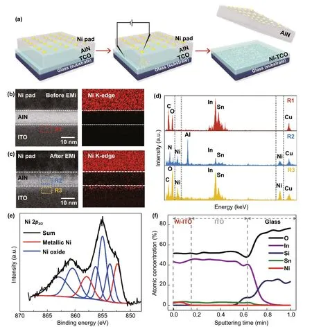
Fig. 1 Metal implantation on the surface of TCOs: a Schematic of EMi process. HR-TEM images and Ni EDS mapping images b before and c after EMi. d EDS spectra measured at R1, R2, and R3 in Figs. 1b and 1c. e XPS core-level spectra of Ni 2p peaks before and after EMi. f Ni, Sn,Si, In, and O concentrations of the Ni-ITO films with respect to the depth from the ITO surface
Figure 1a shows a schematic of the EMi process carried out on a thin film of sequentially deposited TCO (ITO, AZO, or FTO), sacrificial buffer (AlN), and metal (Ni, Ag, or Cu).The sacrificial AlN layer serves not only to protect the TCOs from damage by electric shocks but also to provide a passage for metal ions coming from the metal pad to the TCO layer.When a sufficiently high electric field (> 2.1 MV cm-1) is applied on the metal pads, metal conduction pathways are instantaneously opened, similar to the lightening discharge channel in the AlN layer (Fig. 1a and S1a, b) [28]. The EMi voltage (which is the voltage required to produce conductive doping channels) varies with the buffer layers (Fig.S1c). In this study, the thickness of the TCO layer is set to 30—50 nm, which is much thinner than that of conventional TCOs (150—180 nm). The AlN buffer layer and metal pad are removed after conducting the EMi process. Figure 1b, c shows the high-resolution transmission electron microscopy(HR-TEM) and energy-dispersive X-ray spectroscopy (EDS)images before and after EMi using Ni on ITO. Before EMi,the interfaces between layers are clearly observed; further,Ni is not detected in the AlN and ITO layers (Fig. 1b). By contrast, after EMi, the interfaces between layers become vague, and Ni signals appear in both the AlN and ITO layers(Fig. 1c). The Ni signal observed at the epidermal layer of ITO is the strongest, and this signal decreases and disappears as the depth increases, suggesting that the doped metal ions are predominantly located within the depth of a few nanometers, although some could migrate deeply into the ITO. Figure 1d presents the EDS spectra measured at R1 in Fig. 1b (top spectrum), and R2 and R3 in Fig. 1c (middle and bottom spectra), respectively. Notably, the Ni signal clearly appears in the R3 region, whereas the Ni signal observed in R2 is relatively weaker, and there is no Ni signal in R1. This indicates that the high electric field drives metal ions to the epidermal layer of TCO through the AlN layer [29]. This phenomenon is observed in all EMi results obtained with different metals and TCOs, suggesting the proposed EMi method can be universally applied. This feature is distinguishable from normal doping occurring in semiconductors.The effective penetration depth of EMi, which corresponds to the projection range of ion implantation, can be controlled based on the types of buffer materials and their thicknesses,as well as the electric field magnitude. In this experiment,we used 10-nm AlN as a buffer layer for allm-EMi owing to its lower EMi voltage than other materials such as Al2O3,Si3N4, and SiO2(Fig. S1c) and easy removal by a solvent(CD30 developer). The surface morphology of the TCOs does not critically change after EMi and the removal of the AlN layer (Fig. S2). The wide-scan spectra of X-ray photoelectron spectroscopy (XPS) show that Ni 2ppeaks only appear at the ITO surface after EMi (Fig. S3a), consistent with the EDS results of TEM. From the spectral decomposition of the Ni 2p3/2peak (Fig. 1e), the coexistence of metallic nickel (Ni0; 852.4 and 858.1 eV) and nickel oxides,including nickel hydroxide and its compounds (853.6, 855.0,856.4, 860.8, and 863.5 eV), is revealed [30]. The Ni atom has a smaller atomic radius, greater electron affinity, and higher electron negativity than those of the In atom. In addition, the dissociation energy (396 kJ mol-1) of the Ni—O bond is higher than that (320.1 kJ mol-1) of the In-O bond[18, 31]. Therefore, instead of In-O bond formation, Ni—O bonds are formed by the Ni atoms implanted into the ITO,which is reflected by the variation in the oxygen binding energy, while the change in the In and Sn binding energies is negligible (Fig. S3b—d). Figure 1f shows the variation of atomic concentration, with respect to the etching (= sputtering) time, based on an XPS depth profile. At an etching time of less than 8 s (depth < 10 nm), the atomic percentage of Ni is observed to be 2.5—3 at%, and that of In decreases from ~ 45 to 42 at%, while that of Sn is constantly maintained. As the etching time further increases, Ni disappears and In is saturated until the interface between the ITO and glass substrate is approached. These analyses firmly indicate that the implanted Ni exists as interstitial atoms and substitutes for In within 10 nm from the ITO surface.
3.2 Optical and Electrical Properties of m-TCOs
Thin-film electrodes must have two essential properties—transparency and electrical conductivity; however, these properties are contradictory to each other owing to their inverse proportional relationship. To investigate the effect of EMi on this inverse relation, we examined the transmittance andRSHof the 30- and 50-nm TCOs after the EMi process and performed a comparison with the TCOs before EMi (Fig. 2). In Fig. 2a—c, the transmittance of (a) ITO,(b) AZO, and (c) FTO explicitly increases as the thickness decreases, regardless of the EMi process. AfterNi-EMi, all TCOs show a high transmittance (> 85%) over the entire visible range (400—700 nm), which is lower by less than 2%compared to those of the TCOs before EMi. In particular,the transmittance ofNi-ITO is maintained to be over 80% in the UV range (320—400 nm) (Fig. 2a), while that of Ref. ITO(commercially purchased, 150 nm) sharply decreases to 35%at 320 nm. Similarly,Ag- andCu-ITOs show a high transmittance (> 80%) in the entire visible range (Fig. S4). Notably,regardless of metal dopants,m-ITO commonly shows a high transmittance in the UV to visible range, indicating that it is a prospective electrode for UV optoelectronic devices.
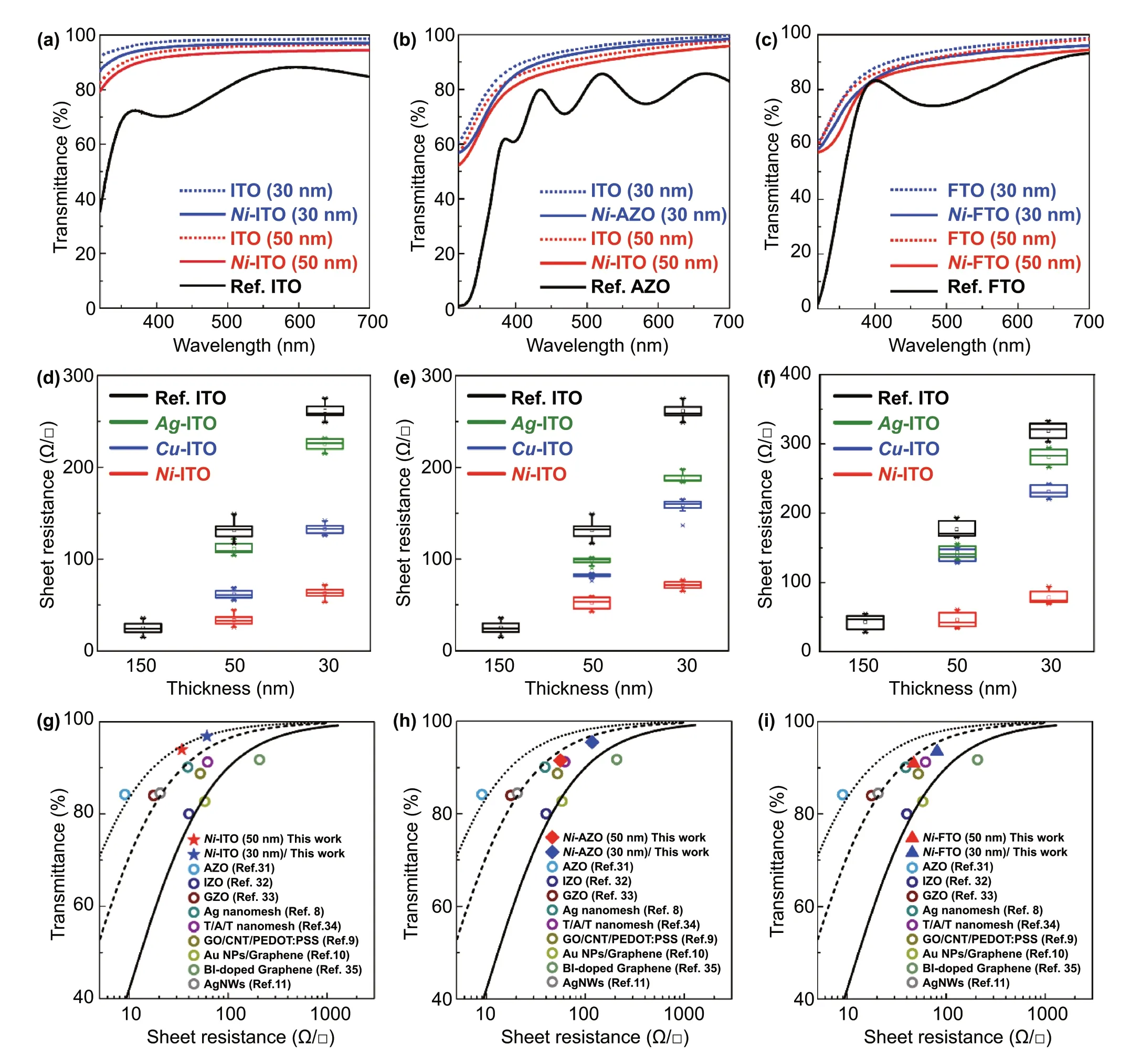
Fig. 2 Transmittance and RSH of m-TCOs: a-c Comparison of UV—visible transparency spectra of a Ni-ITO, b Ni-AZO, and c Ni-FTO. d-f RSH of d m-ITO, e m-AZO, and f FTO depending on the layer thickness. m is Ni (red), Ag (green), and Cu (blue). The black is the reference of each TCO. Transmittance (at 550 nm) as a function of RSH of g m-ITO (solid star symbols), h m-AZO (solid rhombus symbols), and i m-FTO (solid triangle symbols) samples alongside other reference samples. A series of solid and dotted lines represent curves calculated using the Tinkham equation corresponding to σOp/σDC values of 43 (solid line; minimum industry standard), 100 (dash line), and 200 (dotted line)
Furthermore, theRSHofm-TCOs was measured as a function of layer thickness depending on the implanted metals,using the four-point probe method (Figs. 2d—f and S5). TheRSHof TCOs before EMi is inversely proportional to the film thickness, as expected. However, after EMi,m-TCOs show an explicit decrease inRSHcompared to those of TCOs before EMi, although theRSHofm-TCOs increases as the film thickness decreases. Moreover, among three metals (Cu,Ag, and Ni), Ni is the most effective dopant for reducing theRSHby as much as ~ 77% (ITO), ~ 64% (AZO), and ~ 74%(FTO), respectively. TheRSHofNi-ITO, in particular, is as low as 61 ± 10 Ω/□ (30 nm) and 34 ± 11 Ω/□ (50 nm),which is of the same order as theRSHof Ref. ITO (150 nm),namely 26 ± 11 Ω/□ (Fig. 2d). Form-AZO andm-FTO, the lowestRSHis 87 ± 18 and 47 ± 15 Ω/□ forNi-AZO (50 nm)andNi-FTO (50 nm), respectively (Fig. 2e, f). TheRSH,resistivity, and transmittance of theNi-TCOs at 550 nm are listed in Table S1. To further investigate the electrical property of theNi-TCOs, we measured the carrier density and hole mobility (Table S2). The carrier density ofNi-TCOs(Ref. TCOs) is of the order of 1021(1020) cm3, increasing up to ~ 104% inNi-ITO (30 nm). Moreover, the hole mobility ofNi-TCOs shows an almost twofold increment, with the largest value of 26 cm2V-1s-1atNi-ITO (30 nm) compared to those before EMi.
Overall,m-TCOs are less affected by the inverse relation between transmittance andRSH,with respect to the film thickness; further,Ni-EMi is the most effective in tailoring opto-electrical properties of TCOs. This is because the coexistence of metallic Ni and Ni oxide gives rise to some light scattering sites, thereby inducing the enhancement of the light outcoupling intensity (Fig. S6a). In addition, when Ni2+ions are added to In2O3, axial orbitals arising from the splitting of d-orbital (eglevels) of Ni2+impurities are known to exist below the conduction band of In2O and easily undergosp-dhybridization with a relatively lower energy than that in the case of Ag and Cu [32]. In this regard, theeglevels of Ni2+impurities are relatively higher than those of Ag and Cu; therefore, the small reduction in the band gap energy and the expansion of conduction band-like states inNi-ITO may be able to facilitate the charge transport. Furthermore, Ni has a smaller ionic diameter than those of Ag and Cu. This could possibly contribute to the reduction of carrier scattering inNi-ITO, compared toAg- andCu-ITO,via the suppression of oxygen defects [33]. These multiplicative factors increase the electrical performance ofNi-ITO drastically compared to those ofAg- andCu-ITO. Nevertheless, these doped Ni atoms do not significantly change the structural and morphological properties of TCOs, leading to a trivial difference in angle-dependent light outcoupling efficiency of the fabricated device (Fig. S6b).
For a more quantitative analysis of the relationship betweenRSHand transmittance, we calculated the figure of merit (FOM). In general, theRSHand transmittance values of TCOs can be expressed with the Tinkham formula given in Eq. (1):
where σOp(λ) is the optical conductivity (here, at 550 nm)and σDCis the DC conductivity of the film [34]. In this formula, the ratio of σDC/σOpcan be considered as the FOM for the TCOs, as it can provide an intuitive understanding of the relation between theRSHand transmittance of the TCOs.From an industrial perspective, 43.85 (RSH≤ 100 Ω/□ and transmittance at 550 nm ≥ 90%) is commonly regarded as the required minimum FOM value [35]. Figure 2g shows the transmittance (at 550 nm) versusRSHof the 30- and 50-nmNi-ITO (solid star symbols) in comparison with those of the various types of transparent electrodes reported in the literature [6—9, 36—40]. Allm-TCOs (ITO, AZO, FTO)studied here yielded FOM values ranging from 79 to 194(Fig. 2g—i), which exceed the minimum standard σDC/σOpvalue required in the industry. Furthermore, the FOM values of the proposedm-TCOs are much greater than those obtained in other studies.
3.3 Work Function Engineering of m-TCOs
Till date, the direct transition ofn-type TCOs top-type TCOs through surface modification by metal implantation has not been reported, except for surface modification using self-assembled molecules or co-deposition of metals[12—14]. To investigate the possibility of such a transition via EMi, we probed the WF ofm-TCOs using an independent Kelvin probe (KP) microscope and performed a double check using UV photoelectron spectroscopy (Fig. 3 and Table S3). AfterNi-EMi, the WF ofNi-ITO increases up to 5.18 eV (from 4.68 eV before EMi), whereasCu- andAg-EMi on ITO decrease the WF to 4.38 and 4.28 eV,respectively (Fig. 3a). The variations among the WFs of them-ITOs reach up to 0.9 eV, which is remarkable compared to the previous reports [5, 10, 12]. Moreover, the WF values ofNi-,Cu-, andAg-ITO are similar to those of pure Ni(~ 5.17 eV), Cu (~ 4.39 eV), and Ag (~ 4.26 eV), as proven by the KP results, while they are lower than those of nickel oxide (> 5.2 eV) [41], copper oxide (> 5.2 eV) [42], and silver oxide (> 5.26 eV) [43]. This trend is similarly observed inm-AZO (Fig. 3b) andm-FTO (Fig. 3c) with variations depending on TCO types. The WF variation inm-AZO is 0.62 eV, with a minimum WF value of 4.39 eV and a maximum of 5.01 eV, while inm-FTO, it is 0.95 eV, with minimum and maximum WF values of 4.30 eV (Ag-FTO) and 5.25 eV (Ni-FTO), respectively. The WF change of materials(i.e.,Ni-ITO, for example) is closely associated with the doping concentration of the Ni atoms exposed at the surface after the vacancy sites in ITO are occupied, as well as the formation of Ni—O bonds at the surface. As stated previously, Ni atoms injected into ITO can more easily produce a Ni—O bond (compared to the formation of an In-O bond)owing to the smaller atomic radius, greater electron affinity,and higher electron negativity of Ni atoms than those of In atoms. Further, Ni—O bond has a higher dissociation energy(396 kJ mol-1) than In-O bond (320.1 kJ mol-1) [18, 31].Therefore, the size, electron affinity, and electron negativity of doping elements can influence the WF change of materials. This analogy also applies to otherm-TCOs. In addition, the WF ofm-TCOs is affected by the thickness of the TCO layer; however, the variation due to this thickness is not very high (< 0.1 eV); this is because of the low doping concentration (i.e., 2.5%—3% for Ni) in the epidermal layer(within a few nanometers) of TCOs (Table S3). With this tunable WF of TCOs, the energy bands can be well aligned in various energy conversion devices, including LEDs and OPVs. Figure 3d, e schematically shows the electronic band diagrams of OLED and OPV devices, respectively, in which the OLED usesm-TCOs as the anode and an OPV as the cathode. For the fabrication of practical devices,Ni-TCOs will be appropriate as anode electrodes because of the raised WF value (Fig. 3d), whereasAg-TCOs have an advantage as cathodes in OPVs due to the lowered WF value (Fig. 3e).Details on the practical devices usingm-TCOs will be discussed later. On the other hand, we investigated the WF changes of theNi-ITO and Ref. ITO over time to figure out the long-term stability of the TCO after EMi (Fig. S7). The result indicates that well-tailored WF values ofNi-ITO are stably maintained over time.
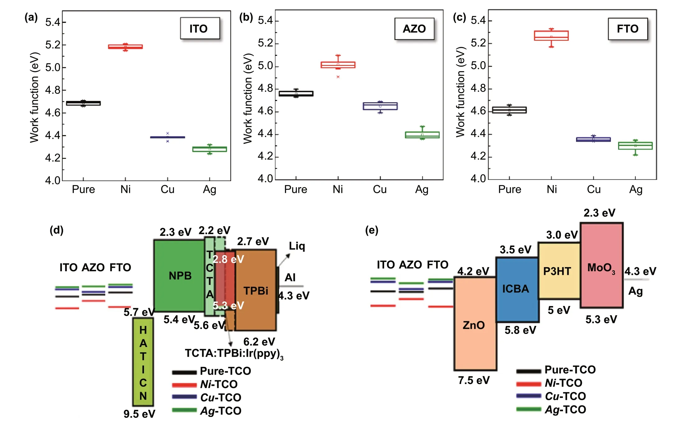
Fig. 3 Work function of m-TCOs: a m-ITO, b m-AZO, and c m-FTO. Schematic energy band diagram of the components that comprise the d OLED and e OPV with the various EMi applied electrodes (Ref. TCO and m-TCO)
3.4 Theoretical Analysis for the Mechanism of Dopant-tunable m-TCOs
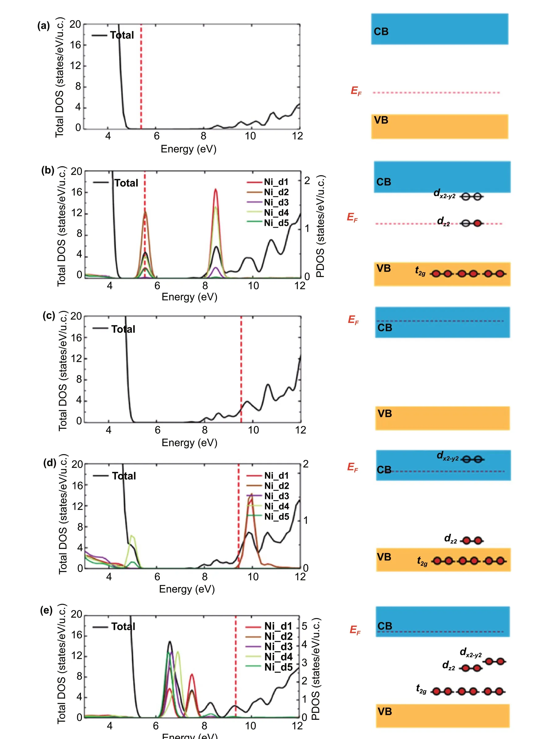
Fig. 4 Theoretical calculation. Total density of states (DOS) and projected density of states (PDOS) onto a Ni atom (left panels) and schematics for defect levels (right panels) for a pristine In2O3 and b In2O3 with a substitutional NiIn defect. Total DOS and PDOS onto an Ni atom (left panels) and schematics for defect levels (right panels) for c Ref. ITO, d ITO with a substitutional NiIn defect, and e ITO with an interstitial NiIn defect
To understand the underlying mechanism by which the WF ofm-TCOs varies, we prototypically investigated the effects ofNi-EMi on ITO using density functional theory (DFT) calculations (Fig. 4) (see Experimental Section for details). Based on the EDS and XPS analyses,the crystal structure (or model) ofm-ITO is given in Fig.S8, wherein metal (i.e., Ni) atoms can substitute In atoms or be interstitially located in the ITO. The generalized gradient approximation (GGA) and the on-site Coulomb correlation (U)functional for the exchange—correlation potential were used to estimate a WF of 4.77 eV for pure ITO [23—25], which agrees well with the measured value(Fig. 4a). When Ni atoms substitute for the In atoms in In2O3, theeglevels of Nid-orbitals lie in the band gap,whereas the inter(non)-axial orbitals arising from the splitting of d-orbital (t2g) levels are located below the valence band maximum (Fig. 4b). At theeglevels, thedz2orbital state is half-filled near the Fermi level, and the unfilleddx2-y2orbital state is located slightly below the conduction band minimum. This indicates that the empty Nidlevels can capture electrons, and consequently, the implanted Ni influences the WF of ITO. Because Sn atoms serve asn-type dopants, the Fermi level is located above the conduction band minimum (Fig. 4c). The Ni substitutional defect decreases the Fermi level by 0.10 eV (from 9.52 to 9.42 eV) because the half-filled Nidz2level captures electrons. This level is subsequently lowered to the valence band edge, as shown in Fig. 4d, whereas the Nidx2-y2level remains empty above the minimum conduction band. By contrast, when Ni creates an interstitial defect, the electron capture effect is more significant, filling all Nidlevels and thereby lowering the Fermi level by as much as 0.18 eV(Fig. 4e). This result supports the idea that the Fermi level can be lowered by Ni-related defects, where the interstitial Ni elements dominantly increase the WF. On the contrary,the interstitial Cu and Ag atoms elevate the Fermi level of ITO, resulting in a decrease in the WF value, as shown in Fig. S9. This decrease might originate from the relatively lower WF and oxidation energy of pure Cu and Ag compared to the WF of ITO, as analyzed in Fig. 3. Further, this is likely caused by the different electronic configurations of Ag and Cu compared to that of Ni. Metallic Ni has two vacant sites for electrons in the 3dorbital, whereas Ag and Cu have fully occupied 3dorbitals. As Ni can accept two electrons, it lowers the Fermi level when it is substituted or interstitially doped in the ITO matrix, leading to an increase in the WF value and enforcing thep-type property of ITO; by contrast, Ag and Cu prefer to donate an electron to the matrix, thereby elevating the Fermi level and causing the matrix to exhibit moren-type characteristics.Consequently, this result elucidates the rationale for the modulation of the WF in TCOs through EMi using various metals.
3.5 Device-Level Validation of m-TCOs as Anode or Cathode Electrodes
Based on these findings, we employedm-ITOs and Ref. ITO as anode (p-) or cathode (n-) electrodes of various types of optoelectronic devices (i.e., OLED, UV LED, and OPV),which require WF-tunable TCOs, to validate the proposed EMi method at the device level. Initially, we fabricated organic green LEDs and inorganic UV LEDs usingNi-ITO as the anode and then inverted OPVs usingAg-ITO as the cathode to confirm the versatility ofm-TCOs. Herein,NiandAg-ITOs were applied to the devices representatively,due to its superior performance than otherm-TCOs. Figure 5 shows schematics and exemplary performances of theNi-ITO based (a, d) OLED (Ni-ITO/OLED) and (b, e) UV LED(Ni-ITO/UV LED), and (c, f)Ag-ITO based OPV (Ag-ITO/OPV).
3.5.1 OLEDs
For the OLED, 30- and 50-nmNi-ITO/OLEDs were fabricated, along with a 150-nm Ref. ITO/OLED for comparison,using a TCTA/TPBi-based green phosphorescent photoactive layer with and without hole injection layer (HIL), as shown in Fig. 5a (see Experimental Section for details). Figure 5d shows the luminance-current density-voltage curves of the 30- and 50-nmNi-ITO/OLEDs. Compared to Ref.ITO/OLED, bothNi-ITO/OLEDs show a higher luminance and current density at driving voltages of 2-8 V. Specifically, the driving voltage of both the 30- and 50-nmNi-ITO/OLEDs at 1000 cd/m is ~ 4.9 V, which is reduced by 15% compared to that of Ref. ITO/OLED. Moreover, the current density in the 30- and 50-nmNi-ITO/OLED at 6 V is ~ 79% and 123% greater, respectively, compared to that in Ref. ITO/OLED. We also measured leakage currents for a reverse voltage sweep from 0 to -5 V. Compared to Ref.ITO/OLED, bothNi-ITO/OLEDs show much lower leakage currents (Fig. S10a), probably due to the reduced surface roughness of thinNi-ITO films (Fig. S2), demonstrating the reliability ofm-TCOs during device operation. A higher current density obtained for the 50-nmNi-ITO/OLED over 30-nmNi-ITO/OLED is attributed to the lowerRSHand higher WF of the 50-nmNi-ITO (Tables S1 and S3). In addition, all luminescence properties (i.e., EL intensity, PE, CE,EQE) ofNi-ITO/OLEDs are found to be superior to those of Ref. ITO/OLED (Fig. S10b-d). In particular, the 30-nmNi-ITO/OLED exhibits a higher luminescence efficiency than the 50-nmNi-ITO/OLED owing to the higher transmittance(or light outcoupling) of 30-nmNi-ITO, as discussed earlier.All device performances of the ITO/OLEDs are summarized in Table S4. Consequently, the improved performance ofNi-ITO/OLED over Ref. ITO/OLED is attributed in part to the increased WF ofNi-ITO, which results in a well-aligned energy level betweenNi-ITO and the NPB-based hole transport layer, as shown in Fig. 3d. The energy-level alignment reduces the hole injection energy barrier, leading to a minimal potential loss and contact resistance. Furthermore, the high transmittance and the relatively lowRSHof the 30- and 50-nmNi-ITOs contribute to maximizing the light extraction and minimizing the electrical loss. Notably,Ni-ITO/OLEDs without HILs shows better performances than Ref.ITO/OLED with a hexaazatriphenylenehexacabonitrile(HAT-CN) HIL (Figs. 5d and S10), which highlights the superiority of the proposed EMi method in organic-based optoelectronic devices.
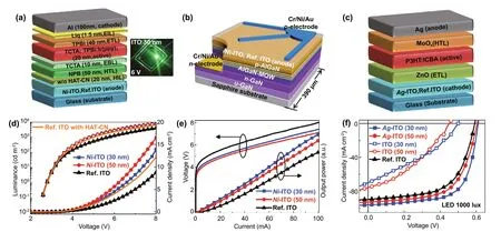
Fig. 5 Organic and inorganic devices using m-ITOs. Geometry (above) and current (density) versus voltage characteristics (below) of a, d OLED, b, e inorganic UV LED, and c, f OPV
3.5.2 UV LEDs
Dopant-tunable ultrathin TCOs are also required for UV LEDs. For the UV LED, inorganic AlGaN is used as photoactive andp-contact layers (Fig. 5b). The direct ohmic contact with thep-AlGaN layer is important owing to the charge injection imbalance caused by the large WF difference between the anode andp-AlGaN layers [44]. When 30- and 50-nmNi-ITOs are used as an anode of the UV LED with ap-AlGaN contact layer, band alignments between layers can be improved owing to the increased WF ofNi-ITO from ~ 4.7 to ~ 5.2 eV. Figure 5e shows the light output power-current—voltage curves of the three UV LEDs plotted up to 100 mA. 150-nm Ref. ITO/UV LED shows the forward voltages of 5.5 V (at 20 mA), whereas the 30- and 50-nmNi-ITO/UV LEDs show forward voltages of 5.0 and 4.85 V,respectively. Note that the current injection efficiency into thep-Al0.1Ga0.9N layer is determined by the electrical properties of the high WFNi- ITO. We also observed the output power increase of 30.9% and 23.3% in the 30- and 50-nmNi-ITO/UV LEDs, respectively, compared to the Ref. ITO/UV LED. EL intensities of the 30- and 50-nmNi-ITO/UV LEDs increase by 30.6% and 22.8%, respectively, compared to that of Ref. ITO/UV LED, as shown in Fig. S11a. The improved light output power and EL intensities are thought to result from much higher transmittance of the 30- and 50-nmNi-ITOs in the UV range (89%—93% at 365 nm),compared to that of 150-nm Ref. ITO (~ 70% at 365 nm).The observed light emission distributions from the 30- and 50-nmNi-ITO/UV LEDs at low (20 mA) and high (50 mA)currents are brighter than the emission from Ref. ITO/UV LED, as shown in Fig. S11b. Compared to Ref. ITO/UV LED, more uniform emission profiles are observed forNi-ITO/UV LEDs at low injection currents, indicating thatNi-ITO is more effective than Ref. ITO in terms of current spreading (or distribution) over the ITO as well as vertical injection. The performances of UV LEDs obtained herein are summarized in Table S5. This performance enhancement is interpreted analogically to that inNi-ITO/OLEDs.
3.5.3 Indoor OPVs
Lastly, in order to further extend the applicability ofm-TCOs, we employedAg-ITOs for OPVs, improving energy level alignment (Fig. 3a, e). In this application,we usedAg-ITO as the cathode (i.e., the electron-collecting electrode) for indoor OPVs to fully utilize its unique features such as ultrahigh transmittance, WF tunability,and low surface roughness. In particular, it is important to maximize light absorption and minimize current loss to achieve a high-power conversion efficiency (PCE)for indoor OPV because of the limited number of incident photons under indoor lighting [45]. Herein,Ag-ITO with a transmittance of 95% at 550 nm and WF ranges of 4.24—4.3 eV was applied as the cathode of inverted OPV,to confirm its validity, as shown in Fig. 5c. Figure 5f shows current density-voltage curves ofAg-ITO/OPVs and Ref.ITO/OPVs. Compared to 150-nm Ref. ITO/OPV, 30- and 50-nmAg-ITO/OPVs show higher PCE owing to the increasedVocandJsc.The increasedVocofAg-ITO/OPVs is attributed to smaller WF values ofAg-ITO compared to that of the Ref. ITO according to metal—insulator—metal model [46]. The improvedJscinAg-ITO/OPVs can be explained by the synergetic effect of higher transmittance(Fig. S4a) and lower WF (Fig. 3a) ofAg-ITO compared to Ref. ITO. Higher transmittance allows more photons to be absorbed in the photoactive layer, generating more charge carriers. In addition, lower WF ofAg-ITO helps to facilitate electron collection and transport via band alignments (Fig. 3e). To highlight the superiority ofAg-ITO/OPVs, the results of 30- and 50-nm pure (without EMi) ITO/OPVs are also plotted in Fig. 5f. These devices exhibit s-shaped current density—voltage characteristics,with reducedVocandJsc, probably due to the insufficient charge transport at the contact layer with ultrathin pure ITOs. The 30- and 50-nm pure ITOs show high resistivity and WF misalignment with ZnO electron transport layer(Tables S1-S3 and Fig. 3e). The photovoltaic parameters of all OPVs are summarized in Table S6.
4 Conclusion
In this study, we proposed novelm-TCOs via electric field-driven metal implantation, through which the WF of ultrathin TCOs could be tailored by as much as 0.97 eV without losses in the surface morphology, crystal structure, and electrical and optical properties. Using thesem-TCOs (e.g.,Ni- andAg-ITOs) as anode or cathode electrodes, we achieved outstanding performance in both organic and inorganic LEDs as well as organic solar cells to verify the universality of the proposed EMi method.These improvements were attributed to the well-aligned energy band at the interface betweenm-TCO and organic/inorganic semiconductor materials, in addition to the ultrahigh transparency in the UV and visible range, lowRSH,and low surface roughness ofm-TCO. This study demonstrates that the proposedm-TCOs can provide a facile and universal solution to the contradiction between transparency and conductivity in ultrathin film-based transparent electrodes, along with full insight into further improvements in state-of-the-art energy conversion devices.
AcknowledgementsThis study was supported by a National Research Foundation of Korea (NRF) grant funded by the Korean government under Grant No. 2016R1A3B1908249. All data are available in the main text and Supporting Materials.
Open AccessThis article is licensed under a Creative Commons Attribution 4.0 International License, which permits use, sharing,adaptation, distribution and reproduction in any medium or format,as long as you give appropriate credit to the original author(s) and the source, provide a link to the Creative Commons licence, and indicate if changes were made. The images or other third party material in this article are included in the article’s Creative Commons licence, unless indicated otherwise in a credit line to the material. If material is not included in the article’s Creative Commons licence and your intended use is not permitted by statutory regulation or exceeds the permitted use, you will need to obtain permission directly from the copyright holder. To view a copy of this licence, visit http:// creat iveco mmons. org/ licen ses/ by/4. 0/.
Supplementary InformationThe online version contains supplementary material available at https:// doi. org/ 10. 1007/s40820- 021- 00735-y.
- Nano-Micro Letters的其它文章
- Recent Advances in Interface Engineering for Electrocatalytic CO2 Reduction Reaction
- Electrochemical Surface Restructuring of Phosphorus-Doped Carbon@MoP Electrocatalysts for Hydrogen Evolution
- Correction to: Boosting Transport Kinetics of Ions and Electrons Simultaneously by Ti3C2Tx (MXene)Addition for Enhanced Electrochromic Performance
- Zeptomole Imaging of Cytosolic MicroRNA Cancer Biomarkers with A Light-Controlled Nanoantenna
- Nanoengineered Shear-Thinning Hydrogel Barrier for Preventing Postoperative Abdominal Adhesions
- Separator Wettability Enhanced by Electrolyte Additive to Boost the Electrochemical Performance of Lithium Metal Batteries