
Scalable fabrication of Bi2O2Se polycrystalline thin film for near-infrared optoelectronic devices applications?
2021-10-28 07:13:52BinLiu劉斌andHongZhou周洪
Chinese Physics B 2021年10期
關(guān)鍵詞:劉斌
Bin Liu(劉斌) and Hong Zhou(周洪)
School of Physics and Electronics,Hunan University,Changsha 410082,China
Keywords: thin films,Bi2Se3,vapor-phase deposition,photodetector,Bi2O2Se
1. Introduction
Two-dimensional(2D)semiconducting layered materials are currently at the forefront of electronic and optoelectronics research because of their numerous desirable properties and are a promising candidate for next-generation integrated circuit technology.[1–5]With only a few years of research,a great number of 2D semiconductors have been isolated or synthesized, including transition metal-dichalcogenides(TMD)[6]and black phosphorus (BP),[7]and other group-VA materials.[8]However, these materials are facing issues towards practical application, such as the need to achieve high carrier mobility,and ambient environment stability.[9–11]MoS2,for example,is a robust TMD material for 2D electronics with tunable bandgap. However, the relatively low carrier mobility (< 200 cm2/V·s at room temperature) hinders its application in high-frequency optoelectronic devices.[12]BP is known for its widely layer-tunable direct band gap(~0.3 eV to~2.0 eV) and relatively high carrier mobility(~1000 cm2/V·s at room temperature).[7]However,the degradation of BP under ambient conditions causes functional failure of devices. Since the electrical performance and stability in the ambient environment are key properties for practical applications, it is necessary to search new, stable 2D semiconductors with superior electronic properties.
Recently, layered bismuth oxyselenide (Bi2O2Se) has been rediscovered as an attractive 2D semiconductor for various applications in electronics and optoelectronics due to its remarkable stability, ultrahigh carrier mobility, and ultrafast broadband photoresponse.[13–17]In addition, Bi2O2Se is also promising for ferroelectric and thermoelectric applications.[18–21]At present, chemical vapor deposition(CVD)is the most widely employed technique for the fabrication of Bi2O2Se,including nanoplates and thin films.[22,23]In most of these reports,randomly distributed Bi2O2Se domains are synthesized on mica substrate and single-crystal Bi2O2Se thin films can be grown on lattice-matched substrates.[24]However,the availability of substrates for large-scale Bi2O2Se growth by CVD has limited its various applications.
In order to avoid this,it is necessary to develop new synthesis methods which could produce large-scale,high-quality Bi2O2Se thin films on diverse substrates,especially on SiO2/Si substrate. In this paper, we present a facile strategy to fabricate large-scale Bi2O2Se thin films by directly conversion of Bi2Se3films in a tube furnace where the oxygen content was controlled. If the Bi2Se3films are directly exposed to air at high temperature,we can only obtain Bi2O3film(see supplementary information: Fig. S1). We attempted to control the oxidation process of Bi2Se3films by gradually decrease the oxygen content to form Bi2O2Se films. Our annealing growth approach ensures the synthesis of Bi2O2Se films on diverse substrates. The photoresponse of these Bi2O2Se thin films are comparable to that of the CVD-grown nanoplate counterparts,with responsivity of 1.7×10⁴A/W and response time of 30 ms.The direct conversion of Bi2Se3thin film to Bi2O2Se thin film at low oxygen concentration on various substrates is a crucial first step towards solving the necessary for scalable and facile synthesis challenge for Bi2O2Se-based integrated electronic and optoelectronic devices.
2. Experimental details
2.1. Synthesis of Bi222Se333 thin films
A ceramic boat containing 0.2-mg Bi2Se3(99.99%,Alfa Aesar) was placed in the center of a horizontal tube furnace equipped with a quartz tube (1 inch, 1 inch=2.54 cm in diameter). The substrates were placed 20-cm downstream from the source powder. The entire system was pumped down to 200 mTorr (1 Torr=1.33322×10²Pa) using a mechanical pump and then flushed with high-purity argon (Ar 99.999%)and the pressure adjusted to 4 Torr. The Ar flow is then adjusted to 90 sccm.After that,the furnace was heated to 580°C in 18 min for the growth of Bi2Se3thin films and maintained at the growth temperature for 20 min. After the synthetic procedure,the furnace was cooled down slowly to room temperature and maintained with gas flow.
2.2. Conversion of Bi222Se333 to Bi222O222Se
The conversion process was performed under controlled atmosphere in a home-built CVD system at atmospheric pressure. The as-synthesized Bi2Se3thin films were placed in the middle of the tube furnace and annealed under low oxygen concentration atmosphere during different periods of time. To control the oxygen concentration inside the system, the furnace tube was first filled with ambient air. Then, high-purity Ar flow was introduced into the furnace at a flow rate of 20 sccm to gradually decrease the oxygen concentration inside the system. After the annealing procedure finished,the quartz tube furnace was switched off. When the furnace reached room temperature,the Ar flow was switched off and the sample was removed.
2.3. Material characterizations
Raman spectra were obtained by using a confocal microscope (Invia-reflex, Renishaw, UK) excited at 633-nm laser.The structure of the films was studied using an x-ray diffractometer (XRD-6100, Shimadzu, Japan). A scanning electron microscopy (SEM) (JSM-6700F, Japan) was used to characterize the uniformity of the morphology and distribution of the sample before and after conversion. Chemical information of the sample is obtained by XPS(AXIS SUPRA,Shimadzu,UK) testing. The optical properties of sample were measured by UV-Vis-NIR spectrophotometer (UV-3600 PLUS,Shimadzu).
2.4. Device fabrication and electrical and optoelectronic properties characterization
The drain and source electrodes of devices were defined by copper grids shadow mask. Subsequently, Cr/Au(10 nm/50 nm) was deposited by thermal evaporation. The back-gated FETs were fabricated on 300-nm thick SiO2/Si substrates, with SiO2as dielectrics and p++Si as gate electrode. The electrical and optoelectronic measurement were carried out with a probe station and an Agilent B2902A source meter under ambient conditions at room temperature. The photoresponse was tested using laser diodes at 520 nm, 650 nm, 780 nm, and 980 nm as incident light. The time-resolved photoresponse was measured using a Tektronix TDS2024C oscilloscope.
3. Results and discussion
The synthetic route for Bi2O2Se thin films involves two steps (Fig. 1(a)). Bi2Se3thin films grown by physical vapor deposition(PVD)approach were used as starting materials for the conversion to Bi2O2Se. The as-grown Bi2Se3thin films were then annealed in a low oxygen atmosphere at 400°C during different periods of time (see Methods section for details). The formation of Bi2O2Se was followed using x-ray diffraction(XRD),as shown in Fig.1(b). The Bi2Se3thin film shows a main peak at 18.56°(2θ), which is characteristic of the Bi2Se3(006) rhombohedral crystal structure.[25]Notably,only(00l)diffraction peaks are observed in the XRD pattern,indicating that the as-grown Bi2Se3film possessesc-axis preferential orientation. After 2-h heat treatment there is clear evidence of the formation of Bi2O2Se from the appearance of XRD peaks at 2θ: 14.80(002),29.54(004),44.82(006),representing the formation of tetragonal Bi2O2Se crystals. After 3 hours,the entire Bi2Se3film is converted to Bi2O2Se.Transmission electron microscopy(TEM)was further performed to clarify the crystal structure and crystallinity of the as-prepared Bi2O2Se film. Figure S2(a) shows a low-magnification TEM image of the Bi2O2Se film. Corresponding high-resolution TEM image is shown in Fig. S2(b). It can be clearly seen that the film presents crystalline grains with different orientations. the lattice spacings of 6.0 °A, 3.7 °A, and 2.8 °A corresponding to the (001), (101), and (110) planes of tetragonal Bi2O2Se. The XRD results and the TEM results confirm the presence of polycrystalline Bi2O2Se films. In a recent study,Bi2SeO5was obtained by treating Bi2O2Se under an oxidation temperature of 370°C–400°C in air.[26]In our study,further increase in the annealing time beyond 3 hours did not lead to form Bi2SeO5phase(see Supplementary-information,Fig.S3),which indicates the oxygen concentration in the furnace is relatively low. Scanning electron microscopy (SEM)was used to study the surface morphology of the Bi2Se3thin films before and after annealing. The as-prepared Bi2Se3thin films have a very smooth surface morphology and appear to be quite dense (Fig. 1(c)). After 3-h annealing, significant morphological changes are observed (Fig. 1(d)). Small crystals grow bigger Bi2O2Se crystals. Significant advantages of this growth method include simplicity and scalability. In particular,the method can be applicable to a range of substrates that can withstand process temperatures of roughly up to 400°C,making it practically applicable in diverse fields. As examples of substrate independence, we have successfully fabricated Bi2O2Se thin films on ITO,mica and sapphire substrates(see supplementary-information, Fig. S4). A clear change in color is observed from brown to light brown,which indicates the complete conversion of Bi2Se3into Bi2O2Se.
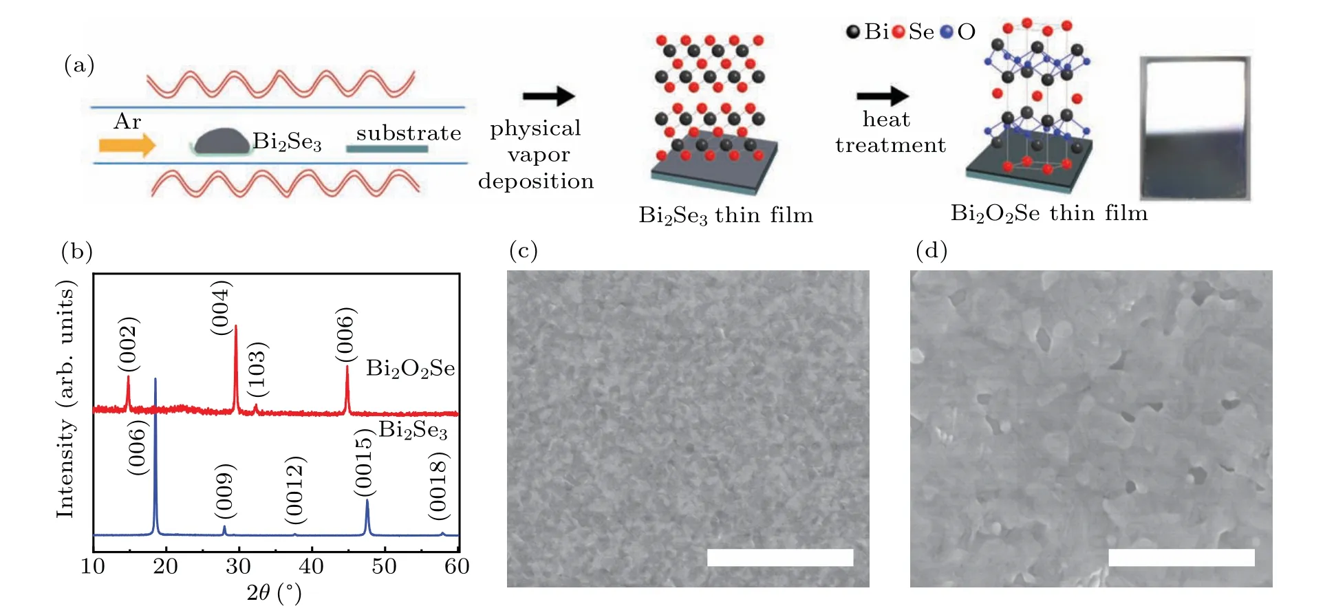
Fig. 1. Fabrication of Bi2O2Se thin films on SiO2/Si substrates. (a) Schematic illustration of the fabrication process of Bi2O2Se thin films using a two-step approach. Bi2Se3 films are deposited using physical vapor deposition technique at 580 °C for 20 min. Then the films are heated at 400 °C for 3 hours at lower oxygen concentration. The photograph shows the fabricated Bi2O2Se film had a mirror-like reflection,indicating high uniformity. (b)Evolution of the XRD patterns as a function of the heat treatment time of the Bi2Se3 film in a low oxygen atmosphere,showing the transformation of phase from rhombohedral structure(Bi2Se3)to tetragonal structure(Bi2O2Se). Top view SEM images of the as-deposited Bi2Se3 film before(c)and after(d)annealing. Scale bar,2μm.
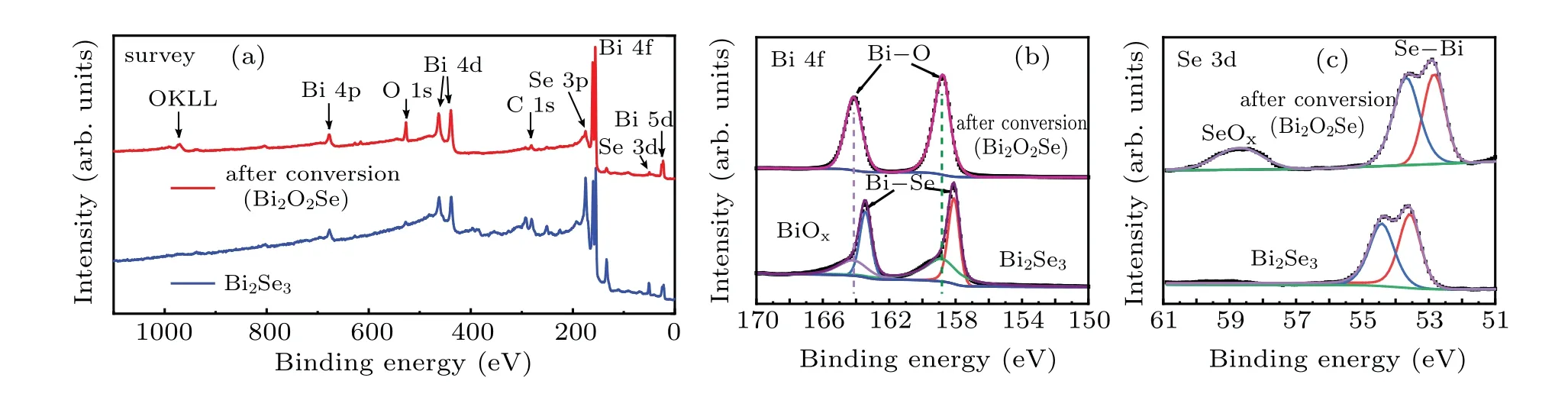
Fig.2. XPS spectra of Bi2Se3 thin film and Bi2O2Se thin film: (a)survey scans,(b)Bi 4f,and(c)Se 3d.
To get further insights into the low oxygen annealing reaction, the x-ray photoelectron spectroscopy (XPS) was carried out on the Bi2Se3thin film deposited on SiO2/Si substrates as well as after reaction for 3 hours under low concentration oxygen. The survey scans of these samples are presented in Fig. 2(a) and the characteristic core level peak of Bi2Se3and Bi2O2Se materials(Bi,O,and Se)are clearly seen.The appearance of a stronger O 1s peak in Bi2O2Se while very weak in Bi2Se3verifies the successful incorporation of O.Further information on the transition from Bi2Se3to Bi2O2Se is analyzed via the bonding state and the elemental composition of bismuth (Bi) and selenide (Se), which is obtained looking at the Bi 4f and Se 3d core level peaks presented in Figs.2(b)and 2(c), respectively. The Bi 4f high-resolution spectrum(Fig. 2(b)) shows two main peaks at binding energy (BE)163.2 eV and 158.7 eV which could be attributed to Bi–Se bonding in Bi2Se3,while those at BE 164.2 eV and 158.9 eV are assigned to Bi–O bonding in Bi2O2Se,respectively.[27]For as-grown Bi2Se3thin films, a bismuth oxide (BiOx) peak is observed, which may exist in the hydroxide form.[28]Correspondingly, the BE of Se 3d peaks have a red shift of about 0.7 eV after annealing for 3 hours (Fig. 2(c)), which may result from the electron sharing between Bi3+and O2?because the Se2?bond only with Bi3+in the Bi2Se3,further indicating the formation of Bi2O2Se. Meanwhile,selenium oxide(SeOx)is also observed after conversion,which indicates the product of the conversion include SeOx.
The conversion of Bi2Se3to Bi2O2Se was also investigated using Raman spectroscopy. Some distinct differences were observed between the two types of samples and the relative motion of the various atoms for these observed phonons is presented in Fig.3(a). For pristine Bi2Se3thin film,two peaks located at 131 cm?1and 174 cm?1are seen, which according to Irfanet al.are characteristic of the Bi2Se3crystal.[29]The first peak refers to the E2gmode and the second one refers to the A21gmode.[30]Noticeably, the Raman spectrum for the Bi2Se3after 3-h reaction time shows only one peak located at 158 cm?1, corresponding to the vibration mode A1gof Bi2O2Se. Raman scattering revealing that Bi2Se3thin film has fully converted to Bi2O2Se thin film after 3-h annealing in the low oxygen concentration. The optical band gap of the asprepared Bi2O2Se thin film was determined using UV-vis-NIR absorbance spectroscopy (Fig. 3(b)). The absorbance spectra of Bi2O2Se thin film have a broad profile and extends to NIR range. The optical band gap of Bi2O2Se thin film is estimated to be 0.85 eV from the corresponding Tauc plot,and the electronic transition is indirect in nature. The band gap energy is slightly higher in energy compared with single crystalline Bi2O2Se nanosheet.
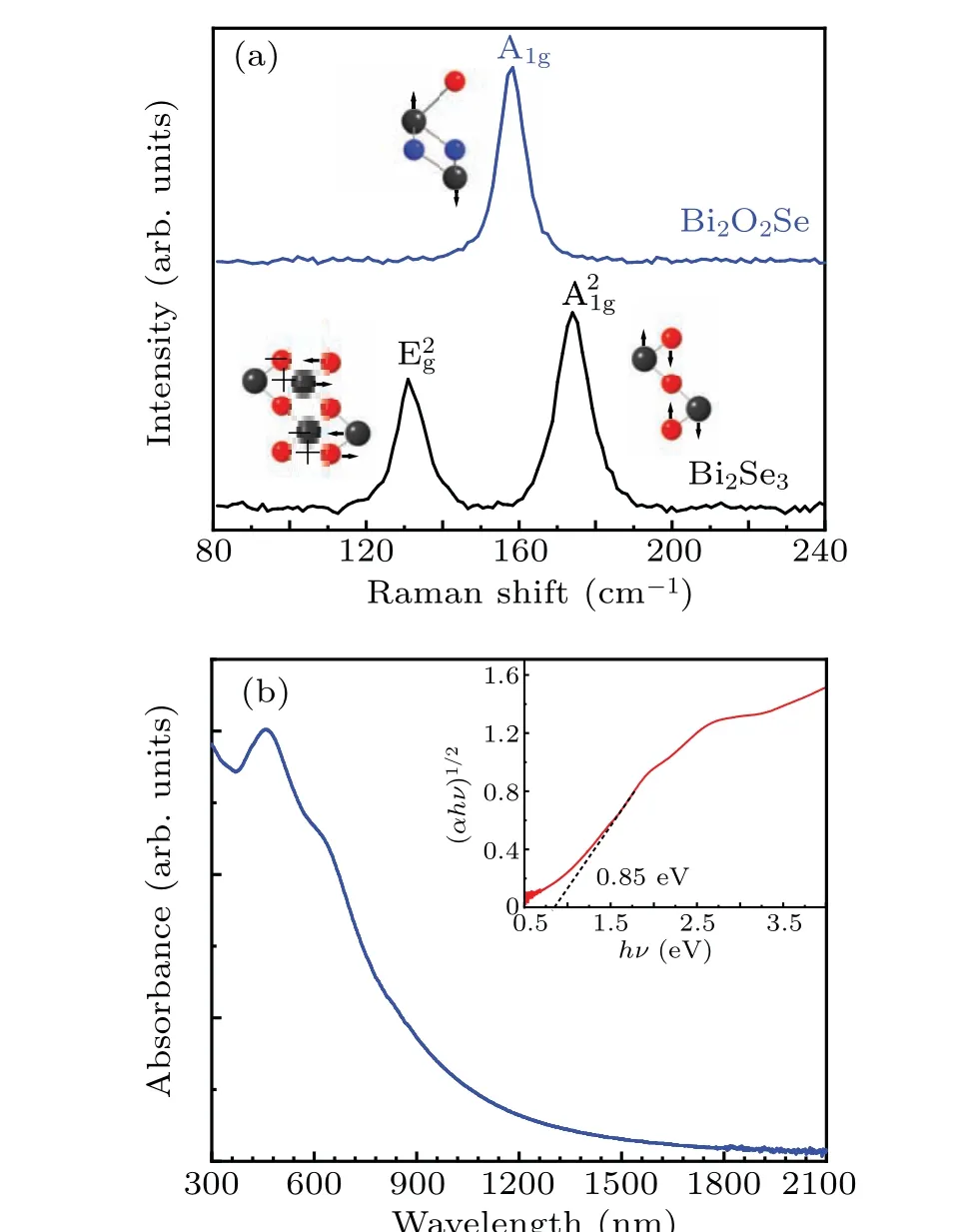
Fig. 3. (a) Raman spectra of as-prepared Bi2O2Se thin film and pristine Bi2Se3 thin film.(b)UV-vis-NIR absorption spectra of as-prepared Bi2O2Se thin film on fused silica substrate. Inset: Tauc plot corresponds to the indirect optical band gaps of 0.85 eV.
To further explore the optoelectronics applications of Bi2O2Se film,the Bi2O2Se photodetectors were fabricated directly on SiO2/Si(Fig.4(a)). Based on large-scale continuous Bi2O2Se thin film,photodetectors arrays were then fabricated.The static resistance measurements of 20 devices indicate the good uniformity of our Bi2O2Se thin film(see supplementary information, Fig. S5). The currentversusvoltage bias (I–V)curves of the as-fabricated Bi2O2Se photodetector in the dark and in the presence of 980-nm lasers with various power densities at room temperature (Fig. 4(b)). The near linearI–Vcurves indicate an ohmic contact between the Bi2O2Se film and the Cr/Au electrodes. Notably,the Bi2O2Se films feature excellent environmental stability, with no apparent change in electrical property after months of exposure in air (see supplementary information, Fig. S6). Furthermore, it can be observed that the Bi2Se2O device exhibits a prominent sensitivity to near-infrared light and the photocurrent improves obviously with the light intensity increasing. The responsivity(R)and detectivity (D?) were calculated to evaluate the photodetection performance of Bi2O2Se-based photodetectors through the following equations:
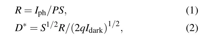
whereIphis defined as the photocurrent subtracted by the dark current,Pis the incident light intensity,Sis the effective illuminated area,D?only considers theIdarkas the major source of shot noise,qis the electronic charge. The light intensity-dependent responsivities at 5-V bias, which reveal that such a photodetector owns a maxRandD?,were calculated to be 1.7×10⁴A/W and 3.9×10¹²Jones(1 Jones=1 cm·Hz1/2·W?1)under 980-nm light at a low light intensity of 0.001 mW/cm2(Fig. 4(c)). TheRvalue of the Bi2O2Se film is slightly smaller than that of their single crystal counterparts previously reported.[31,32]Besides,figure 4(c)demonstrates that the responsivity of the device decreases with the increase of incident power densities, which is due to enhanced scattering or recombination rate of hot carriers as their density increases at higher laser power.[33]
We next studied the response speed of Bi2O2Se film photodetector. Time-dependent photocurrents of the device is displayed in Fig. 4(d), which are operated by periodically turning on and off 980-nm light at a bias of 5.0 V. It can be seen that our device exhibits excellent repeatability, which is suitable for long-term, reliable, and highly sensitive NIR detection/monitoring. A complete on/off cycle in which the photocurrent reveals a fast rise/fall state(Fig.4(e)). The response time(τrise)and decay time(τfall)of the device are estimated to be~89 ms and~30 ms,respectively. The fast response feature is emanated from the high crystalline quality of Bi2O2Se film we obtained. The electrical photoresponse variation of the Bi2O2Se photodetector for varying incident wavelengths at 5-V bias(Fig.4(f)). Qualitatively,the photoresponse has a similar wavelength dependence,indicating the realization of a wavelength selective photodetection.
To investigate the electrical transport characteristics of the Bi2O2Se film, back-gate FETs were fabricated. As shown in Fig.5(a), it can be seen from the output characteristic curves of different back-gate voltages that the source–drain currentIdsvaries linearly with the biasVdsin the range of 0 V–2 V,indicating that a good ohmic contact is formed between the metal electrode and Bi2O2Se film. Figure 5(b) shows the transfer curves of the Bi2O2Se film at various bias voltage of 0.5 V–3 V, which indicate typical n-type behavior. The calculated average carrier mobilities of the sample is 17 cm2/V·s,which is lower than that of the single-crystalline Bi2O2Se.[24,34]WithVdsincreasing from 0.5 V to 3 V, the on-state current can be improved from 2.6×10?5A to 1.8×10?4A. The maximum current on/off ratio (Ion/Ioff) is nearly three orders of magnitude,which is lower than that of recently reported single crystalline Bi2O2Se nanoplate transistors.[31,35]Furthermore, the subthreshold swing is deduced to be 1230 mV/dec. The relatively lower carrier mobility and current on/off ratio are likely limited by the structural defect, such as the grain boundary observed by TEM. The annealing conditions of Bi2Se3films needs to be studied further for improvement of Bi2O2Se films with better crystallographic quality.
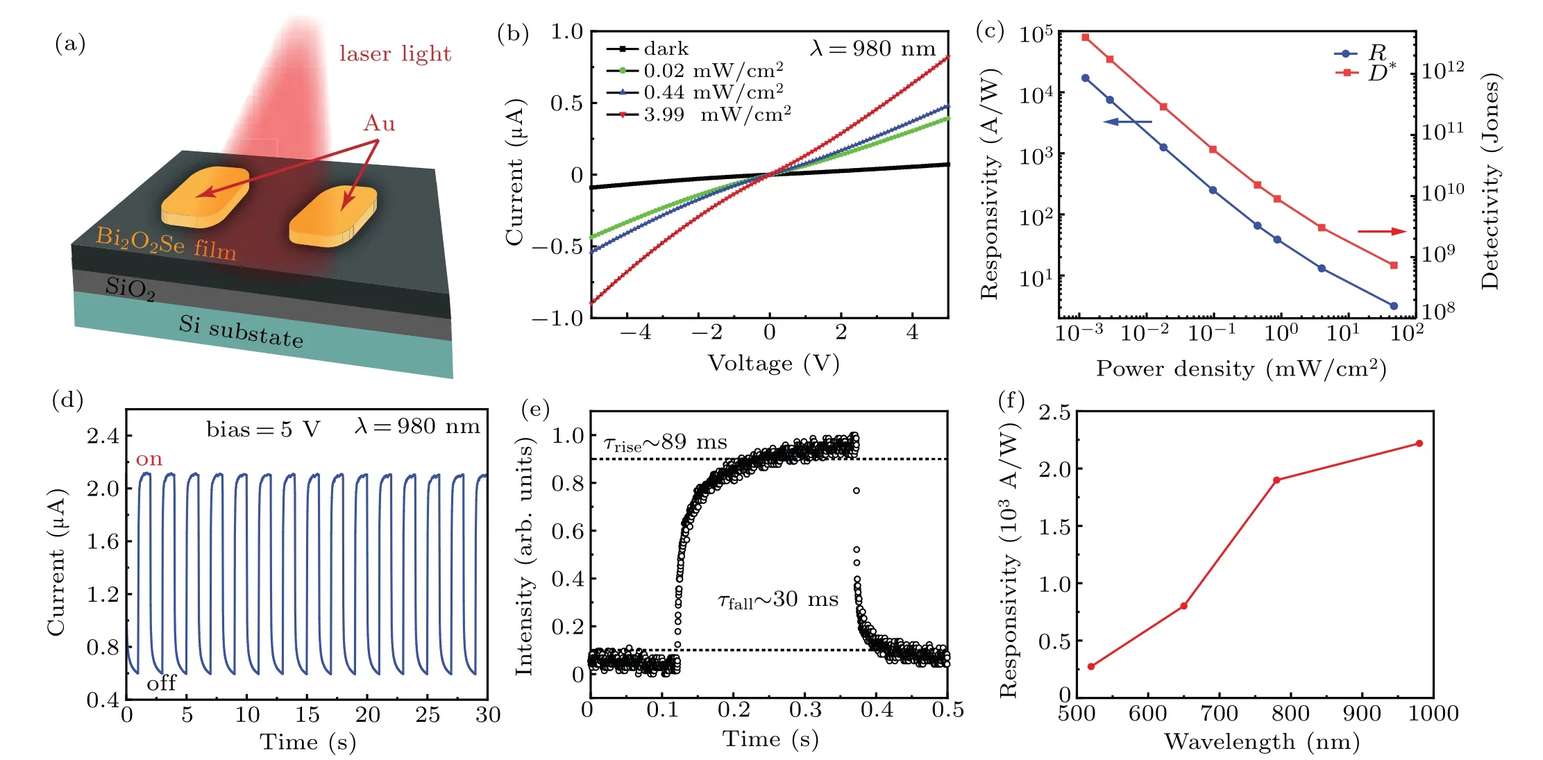
Fig.4.(a)A schematic diagram of the Bi2O2Se thin film photodetector on a SiO2/Si substrate.(b)I–V curves of the Bi2O2Se photodetector as a function of light intensity ranging from 0.02 mW/cm2 to 3.99 mW/cm2 (at 980 nm). (c) The plot of photoresponsivity detectivity and D?versus illumination light intensity at 5 V.(d)Reproducible on/off switching illuminated by 980-nm light at a bias of 5 V.(e)Transient response under the illumination of a 980-nm light. (f)The wavelength-dependent photoresponse of the Bi2O2Se photodetector at 5-V bias.
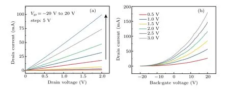
Fig.5. (a)Output characteristics and(b)transfer characteristics of a back-gated Bi2O2Se thin film FET measured at room-temperature.
4. Conclusion
In summary, we reported a new approach to grow largearea 2D semiconducting Bi2O2Se thin films on a wide range of substrates. The prepared Bi2O2Se devices exhibited excellent air stability and comparable quality to single-crystalline Bi2O2Se with responsivity of 1.7×10⁴A/W and response time of 30 ms. All these results reveal that the developed synthesis method can be applied to directly grow Bi2O2Se on other highκdielectrics and opens up the possibility of on-chip fabrication of high-mobility optoelectronic devices with Bi2O2Se.
猜你喜歡
河南科技(2022年8期)2022-05-31 22:28:08
Chinese Physics B(2021年3期)2021-03-19 03:19:50
Acta Mathematica Scientia(English Series)(2020年5期)2020-11-14 11:28:54
考試與評(píng)價(jià)·八年級(jí)版(2020年3期)2020-11-02 02:39:24
學(xué)苑創(chuàng)造·A版(2019年8期)2019-08-15 01:27:21
東坡赤壁詩(shī)詞(2018年4期)2018-11-07 11:01:44
Acta Mathematica Scientia(English Series)(2018年2期)2018-05-05 07:09:39
藝術(shù)生活-福州大學(xué)廈門(mén)工藝美術(shù)學(xué)院學(xué)報(bào)(2016年4期)2016-07-31 19:43:28
水動(dòng)力學(xué)研究與進(jìn)展 B輯(2015年6期)2015-12-01 02:12:18
中學(xué)化學(xué)(2015年5期)2015-07-13 07:34:35

- Chinese Physics B的其它文章
- Physical properties of relativistic electron beam during long-range propagation in space plasma environment?
- Heterogeneous traffic flow modeling with drivers’timid and aggressive characteristics?
- Optimized monogamy and polygamy inequalities for multipartite qubit entanglement?
- CO2 emission control in new CM car-following model with feedback control of the optimal estimation of velocity difference under V2X environment?
- Non-peripherally octaalkyl-substituted nickel phthalocyanines used as non-dopant hole transport materials in perovskite solar cells?
- Dual mechanisms of Bcl-2 regulation in IP3-receptor-mediated Ca2+release: A computational study?